Close Menu
  • Analog Design
    • Latest Analog Layout Interview Questions (2025)
  • Digital Design
    • Digital Electronics Interview Question(2025)
    • Top VLSI Interview Questions
  • Physical Design
    • Physical Design Interview Questions for VLSI Engineers
  • Verilog
    • Verilog Interview Questions(2024)
  • Forum
Facebook Instagram YouTube LinkedIn WhatsApp
SiliconvlsiSiliconvlsi
Ask Questions Register in Forum Login in Forum
Facebook Instagram YouTube LinkedIn WhatsApp
  • Analog Design
    • Latest Analog Layout Interview Questions (2025)
  • Digital Design
    • Digital Electronics Interview Question(2025)
    • Top VLSI Interview Questions
  • Physical Design
    • Physical Design Interview Questions for VLSI Engineers
  • Verilog
    • Verilog Interview Questions(2024)
  • Forum
SiliconvlsiSiliconvlsi
Home»VLSI Design»Why is the substrate in NMOS connected to Ground and in PMOS to VDD?
VLSI Design

Why is the substrate in NMOS connected to Ground and in PMOS to VDD?

siliconvlsiBy siliconvlsiJune 24, 2023Updated:June 28, 2025No Comments2 Mins Read
Facebook Pinterest LinkedIn Email WhatsApp
Share
Facebook Twitter LinkedIn Pinterest Email
NMOS connected to Ground and in PMOS to VDD

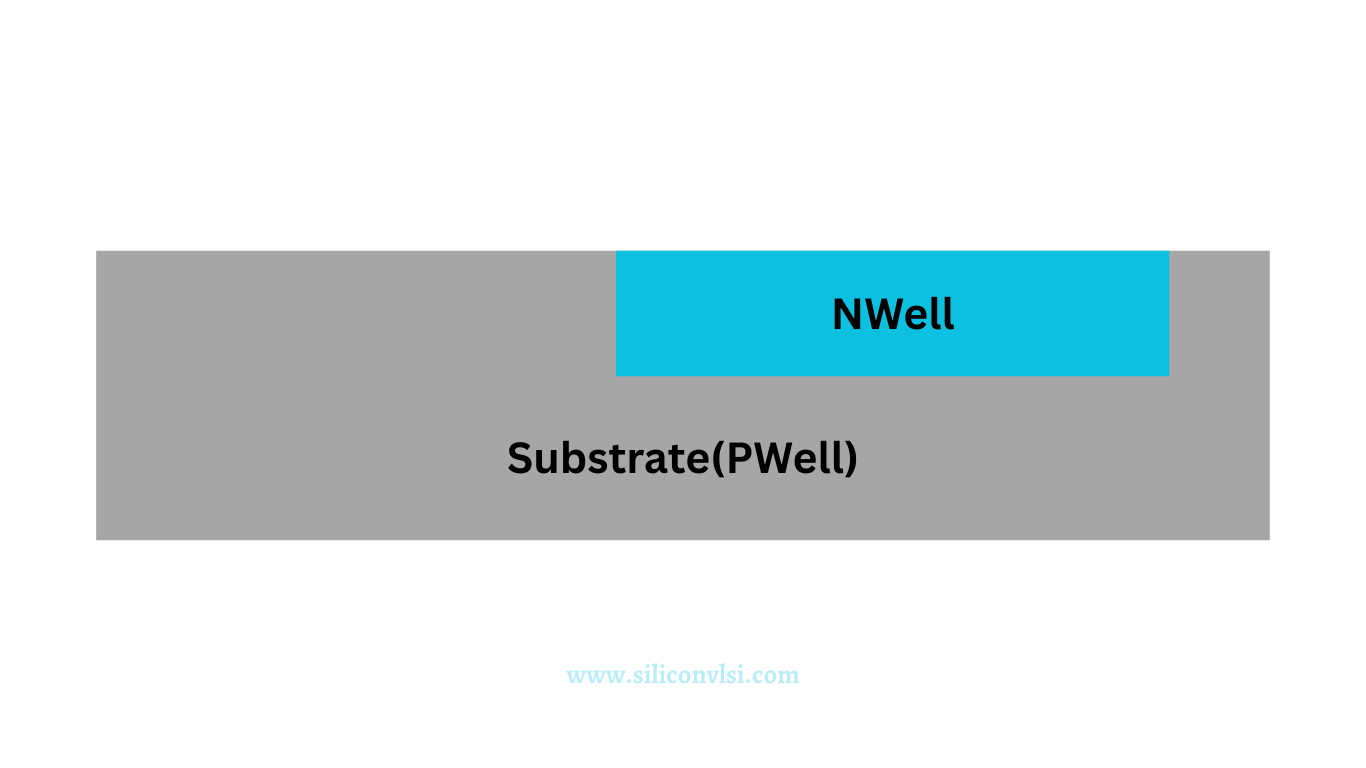
In CMOS (Complementary Metal-Oxide-Semiconductor) logic design, the substrate connection for NMOS (N-channel Metal-Oxide-Semiconductor) and PMOS (P-channel Metal-Oxide-Semiconductor) transistors serves specific purposes. The substrate in NMOS transistors is connected to the ground (0V) because these transistors become active when the voltage between the gate and substrate is positive. By grounding the substrate, the NMOS transistor can operate effectively when the gate voltage exceeds the threshold voltage.

Conversely, in PMOS transistors, the substrate is connected to VDD (the positive power supply voltage). PMOS transistors are active when the voltage between the gate and substrate is negative. By connecting the substrate to VDD, the PMOS transistor can function properly when the gate voltage is lower than the threshold voltage.

The substrate connection establishes the appropriate voltage reference for each transistor type, enabling them to perform their intended functions within a CMOS circuit. By employing different substrate connections for NMOS and PMOS transistors, the CMOS logic design ensures correct operation and facilitates the complementary behavior required for effective CMOS circuitry.

Why Do All NMOS Transistors Share a Common Substrate?

You use a common substrate for all NMOS transistors because the substrate can only be biased to one voltage. Even though this causes a body effect that slows down the transistors and makes them deviate from the ideal MOS current equation, there’s no practical alternative.

NMOS common substrate
Share. Facebook Twitter Pinterest LinkedIn Tumblr Email

Related Posts

How Shielding Avoids Crosstalk Problem? What Exactly Happens There?

September 22, 2024

Navigating the Challenges of Gate Dielectric Scaling in MOS Transistors

August 1, 2024

Challenges in Modern SoC Design Verification

April 20, 2024
Leave A Reply Cancel Reply

Facebook X (Twitter) Instagram Pinterest Vimeo YouTube
  • About Us
  • Contact Us
  • Privacy Policy
© 2025 Siliconvlsi.

Type above and press Enter to search. Press Esc to cancel.