
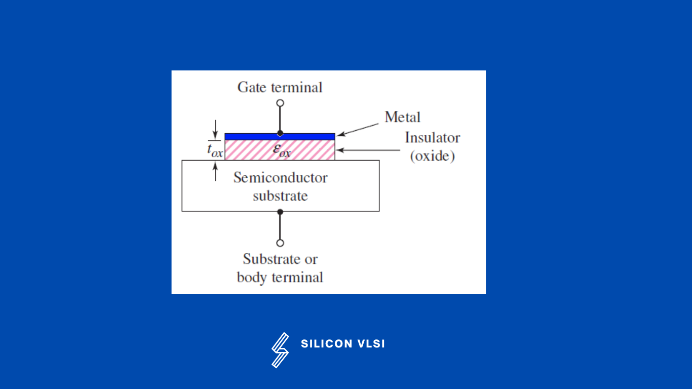
Two-Terminal MOS Structure
The heart of the MOSFET is the metal-oxide-semiconductor capacitor shown in Figure 1. The metal could be made of aluminum or another metal. Most frequently, a layer of high-conductivity polycrystalline silicon is formed on the oxide to replace the metal. However, when referring to MOSFETs, the word “metal” is still frequently used. The parameter tox in the illustration represents the oxide’s thickness. The physics of the MOS structure can be explained with the aid of a simple parallel-plate capacitor.
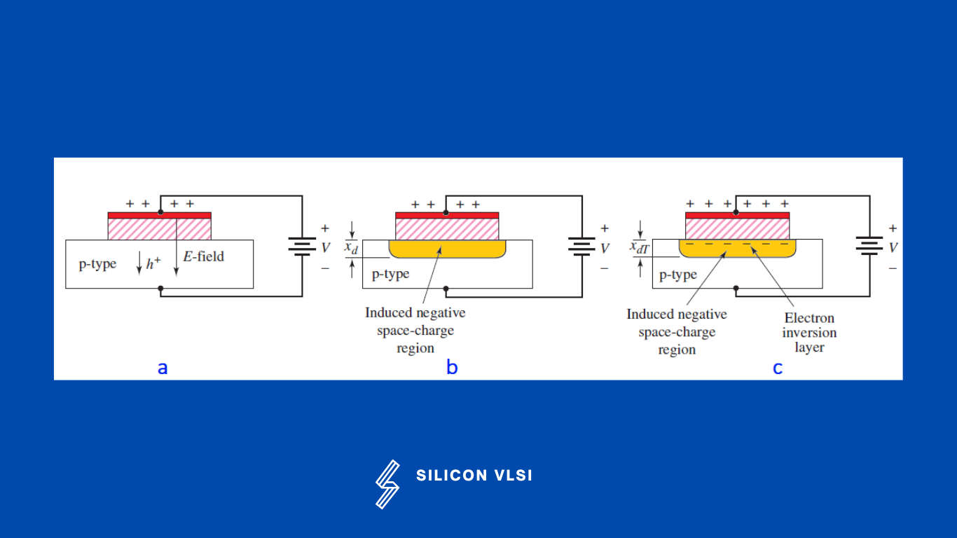
The MOS capacitor with a p-type substrate
Figure 2(a) shows the MOS capacitor. A positive charge now exists on the top metal plate and the induced electric field is in the opposite direction, as shown in the figure. In this case, if the electric field penetrates the semiconductor, holes in the p-type material will experience a force away from the oxide-semiconductor interface.
Now as the holes are pushed away from the interface, a negative space-charge region is created, because of the fixed acceptor impurity atoms. The negative charge in the induced depletion region corresponds to the negative charge on the bottom “plate” of the MOS capacitor.
Figure 2(b) shows the equilibrium distribution of charge in the MOS capacitor when we applied the same small voltage to the gate. When a larger positive voltage is applied to the gate, the magnitude of the induced electric field increases.
Minority carriers called electrons in this case are attracted to the oxide semiconductor interface, as shown in Figure 2(c). This region of minority carrier electrons is called an electron inversion layer. The magnitude of the charge in the inversion layer is a function of the applied gate voltage. #
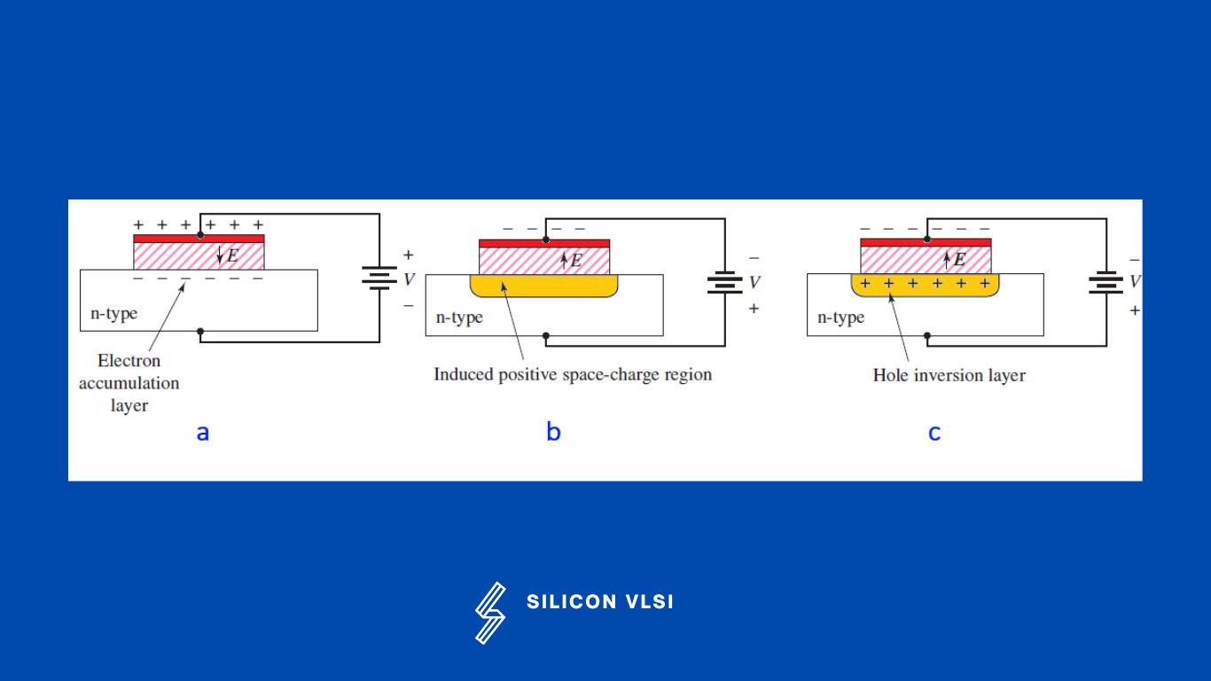
The MOS capacitor with an n-type substrate
The same charge distributions can be obtained in a MOS capacitor with an n-type semiconductor substrate. Figure 3(a) shows this MOS capacitor structure, with a positive voltage applied to the top gate terminal. After this positive charge is created on the top gate and an electric field is induced in the direction shown. In this situation, an accumulation layer of electrons is induced in the n-type semiconductor.
Figure 3(b) shows the case when a negative voltage is applied to the gate terminal. A positive space-charge region is induced in the n-type substrate by the induced electric field. When a larger negative voltage is applied, a region of positive charge is created at the oxide-semiconductor interface, as shown in Figure 3(c). This region of minority carrier holes is called a hole inversion layer.
The magnitude of the positive charge in the inversion layer is a function of the applied gate voltage. This is also called a PMOS. Generally, we called the n-type substrate NWELL. Generally, we use n well in P-substrate for CMOS technology because The mobility of the electronics is much faster than the hole, so by NPN or NMOS, you can get a higher frequency in a much easier way. #
What is Enhancement mode?
The Enhancement mode MOSFET is equivalent to the normally open switch. Voltage must be applied to the gate to create the inversion charge, this transistor is called an enhancement-mode MOSFET #
What is the Depletion mode?
The Depletion mode means that a channel exists even at zero gate voltage. A negative gate voltage must be applied to the n-channel depletion-mode MOSFET to turn the device off #
What is Field Oxide?
Field oxide is deposited outside the area in which the metal interconnect lines are formed. Usually, polysilicon with high doping levels serves as the gate material. Although a MOSFET’s actual structure may be somewhat complicated, the simplified figure can be utilized to determine the fundamentals of a transistor.