
Polysilicon used as a gate contact instead of metal in CMOS
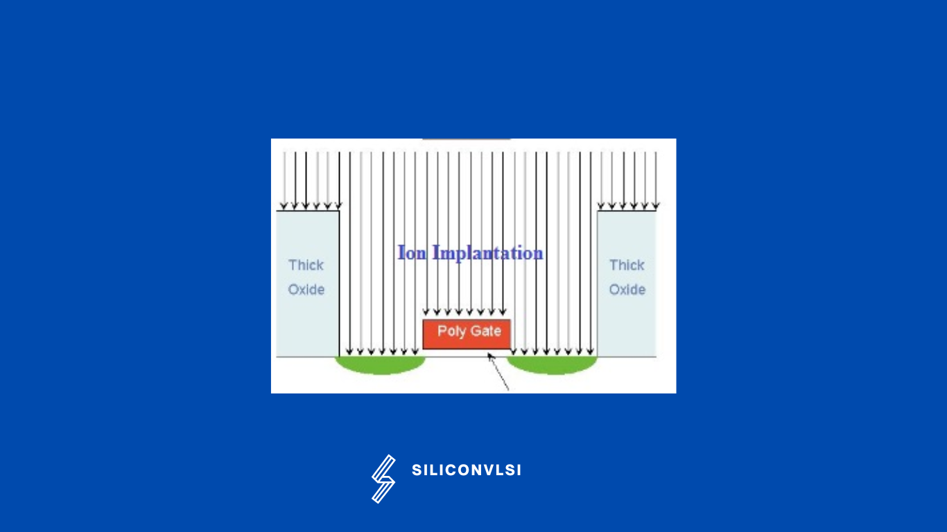
The polysilicon gate acts as a mask for the source and drains implantation during the fabrication process, as it is also called as “Self-aligned Gate Process”.
The doping process of the drain and source requires very high-temperature annealing methods ( above 800°C). If Al is used as a gate material, it would melt under such a high temperature. This is because the melting point of Al is approximately 650°C. But, if polysilicon is used as a gate material, it would not melt. Thus, the self-alignment process is possible with a polysilicon gate.
Earlier, metal gates were used when operating voltages were in the range of 3-5 volts. But, as the transistors were scaled down, the operating voltage also came down. so with that threshold, Vt also came down. Using metal as gate material resulted in a high threshold voltage compared to polysilicon since polysilicon would be of the same or similar composition as the bulk-Si channel. Also, using polysilicon as a semiconductor, its work function can be modulated by adjusting the level of doping.
Poly-Si Gate Electrodes in CMOS Technology
Poly-Si gates have replaced metal gates in metal oxide semiconductor (MOS) transistor technology primarily because they are compatible with self-aligned processes. These processes enable gate doping and the formation of the source and drain in a single ion implantation step. Additionally, the work function of poly-Si gates is only slightly different from that of the silicon substrate, allowing metal oxide semiconductor field effect transistors (MOSFETs) with nearly zero threshold voltage to be realized. This enables aggressive downscaling with fewer voltage and field constraints. Furthermore, both p-type and n-type poly-Si gates are used to create PMOS and NMOS transistors with complementary threshold voltages. Lastly, poly-Si gates can withstand subsequent high-temperature processing steps and can be oxidized, facilitating the fabrication of isolated multi-layer ULSI structures.