
Difference between the metal gate and polysilicon gate technology
The main difference between the metal gate and the polysilicon gate is the resistive material and sensitivity to temperature. Polysilicon gates can bear high temperatures while metal gates can melt over that same temperature, so we can use the polysilicon gates as a self-alignment gate process during the fabrication of CMOS. another reason we can say that Polysilicon gates were favored is that the material could be easily matched to the SiO2 lattice constant.
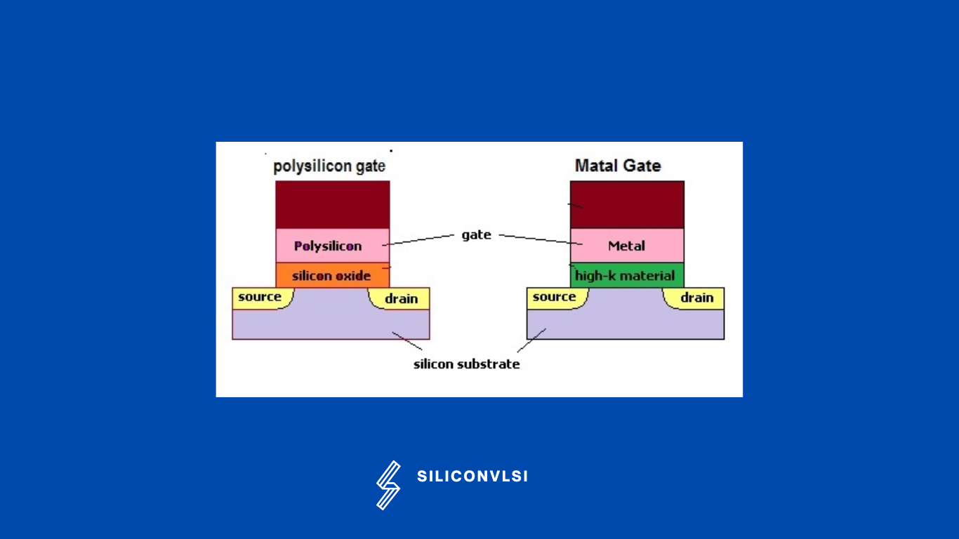
Why is polysilicon used as a gate contact instead of metal in CMOS?
Two main reasons were behind this transition to using polysilicon as a gate nowadays
Self-aligned Gate Process
During the fabrication process, if the gate mask is misaligned, it creates a parasitic overlap of input capacitance Cgd and Cgs. Due to these parasitic, there is a reduction in the transistor’s switching speed. so to avoid that, One of the solutions to the misalignment of the gate mask is what is known as a “Self-aligned Gate Process”.
Now if we use polysilicon, then this poly(polysilicon), acts as a mask for the doping process preventing further doping under the gate region. So, this process makes the gate self-aligned with respect to the source and drain. As a result of all this, the source and drain do not extend under the gate. Thereby reducing Cgd and Cgs.
Very high-temperature annealing processes (over 800°C) are required for the doping process of the drain and source. Al would melt if utilized as a gate material at such a high temperature. This is due to aluminum’s near 660°C melting temperature. However, polysilicon would not melt if employed as a gate material. The polysilicon gate makes the self-alignment procedure possible.
“We can not use the metal gate as a Self-aligned Gate Process because it can not withstand high temperature, during source and drain formation.”
Operating voltages
In contrast to polysilicon, which would have the same or similar composition as the bulk-Si channel, using metal as the gate material produced a high threshold voltage. Additionally, because polysilicon is a semiconductor, the amount of doping can be changed to alter the material’s work function. With Poly, we can get low operating voltage.