
LDD (Lightly Doped Drain) and Halo Doping are two techniques used in semiconductor device fabrication, particularly in MOS (Metal-Oxide-Semiconductor) transistor technology. They are employed to improve device performance and characteristics. Here are the key differences between LDD and Halo Doping:
What is LDD (Lightly Doped Drain)?
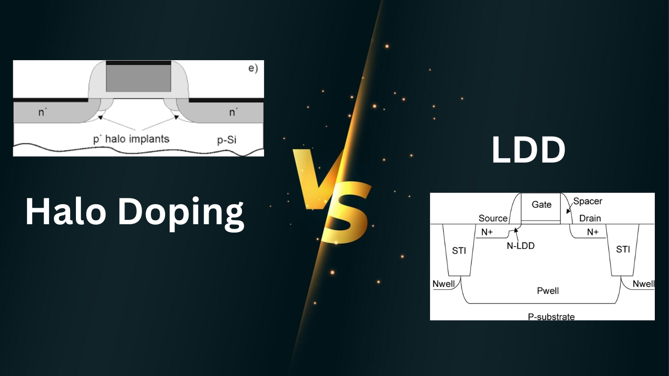
The LDD structure, which spreads the high field at the drain pinch-off area and lowers the maximum field intensity, is studied. It involves introducing thin, self-aligned n-regions between the channel and the n + source-drain diffusions of an IGFET.
What is Halo Doping?
Halo Doping, often referred to as punch-through suppression or “pocket” implants, prevents the source and drain of short-channel devices from being punched through the bulk substrate.
Differences between LDD(lightly doped drain) & Halo Doping
| Aspect | LDD (Lightly Doped Drain) | Halo Doping |
|---|---|---|
| Purpose | LDD is primarily used to reduce the electric field near the drain region of an MOS transistor, preventing hot electron effects and improving device reliability. | Halo doping is used to modify the threshold voltage and control the channel length of an MOS transistor, influencing its performance characteristics. |
| Location of Dopant | In LDD, the lightly doped region is typically located near the drain of the transistor, reducing the electric field at this critical area. | Halo doping involves adding dopants around the channel region of the transistor, affecting the behavior of carriers in the channel. |
| Dopant Concentration | LDD regions have a relatively lower dopant concentration compared to the source and drain regions. They are lightly doped. | Halo doping introduces dopants of varying concentrations to create regions of different doping levels, influencing threshold voltage and channel length. |
| Effect on Transistor Behavior | LDD reduces the electric field near the drain, preventing impact ionization and hot electron effects. It improves device reliability. | Halo doping affects the threshold voltage and channel length, which in turn impacts the transistor’s performance, such as speed, leakage current, and subthreshold swing. |
| Applications | LDD is commonly used in technologies where reliability is a major concern, such as CMOS (Complementary Metal-Oxide-Semiconductor) integrated circuits. | Halo doping is used to control the threshold voltage and channel length in various MOS transistor types, including PMOS (P-channel MOS) and NMOS (N-channel MOS), for optimizing device performance. |