

What is Ohmic Contact?
A metal-semiconductor contact is formed when a metal is connected directly to a semiconductor such as silicon. This interface is extremely important in semiconductor devices because current must flow between the semiconductor and the metal with as little unwanted resistance as possible.
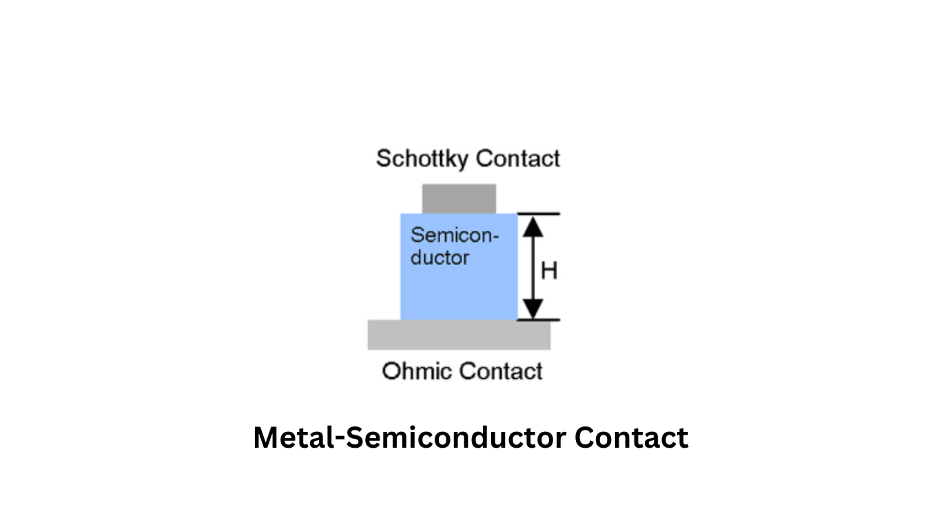
Depending on the materials, doping concentration, and interface properties, a metal-semiconductor junction can behave either as a rectifying contact (Schottky contact) or as a non-rectifying contact (ohmic contact).
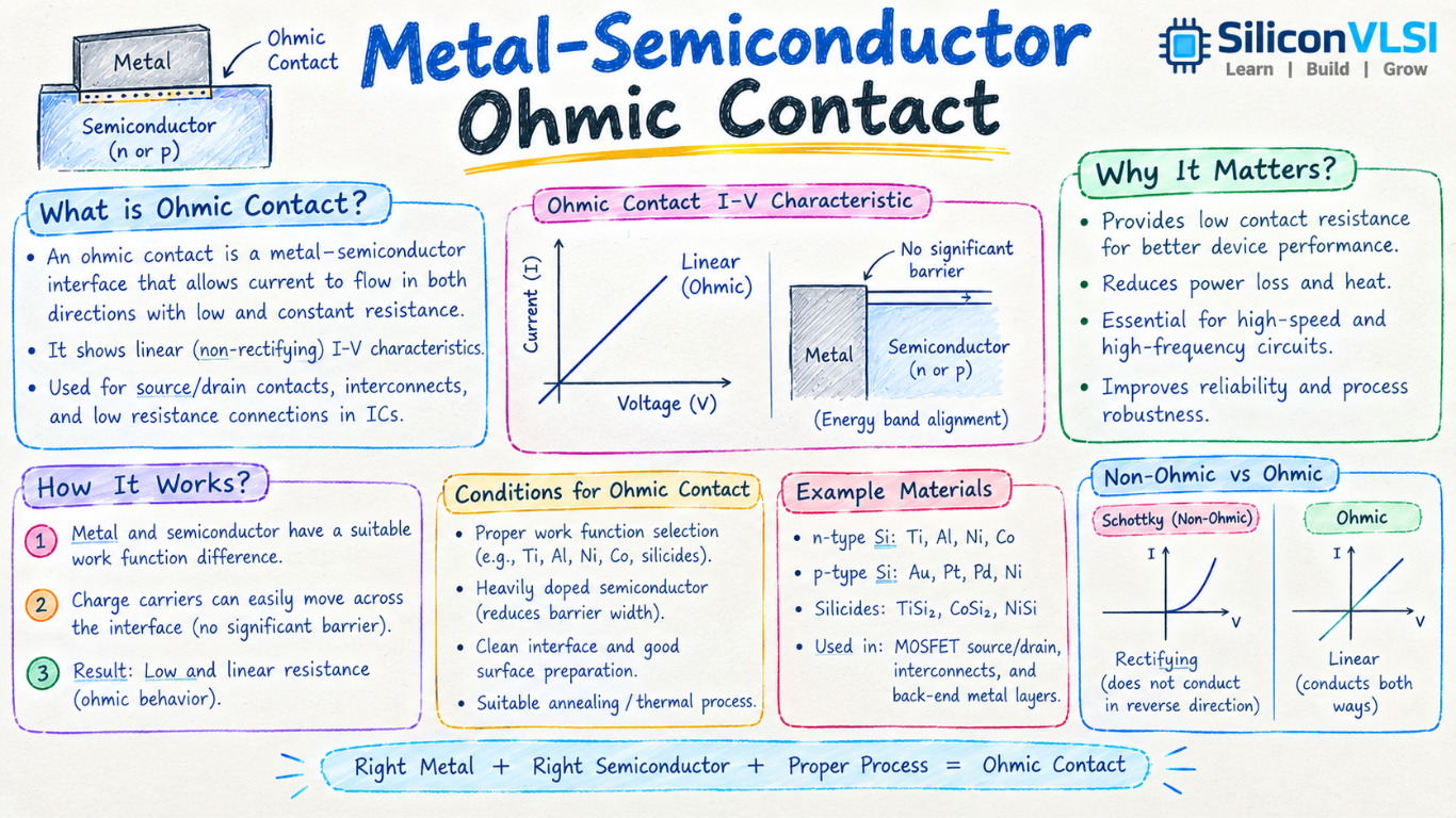
An ohmic contact is designed to provide a low-resistance path for current in both directions, with an approximately linear current-voltage (I-V) relationship over the intended operating range.
What Is a Metal-Semiconductor Ohmic Contact?
A metal-semiconductor ohmic contact is an electrical connection between a metal and a semiconductor that allows charge carriers to flow with low resistance.
The ideal behavior is approximately described by Ohm’s law:
V = IR
where:
- V is the voltage across the contact
- I is the current through the contact
- R is the contact resistance
Unlike a rectifying Schottky contact, an ohmic contact is intended to conduct current without significant diode-like rectification.
The actual contact behavior depends on factors such as semiconductor doping, metal work function, interface states, temperature, and fabrication conditions.
Why Does a Metal-Semiconductor Contact Form a Barrier?
When a metal comes into contact with a semiconductor, charge redistribution can occur because the two materials have different electronic properties.
This can produce band bending and, depending on the material combination and semiconductor type, a potential barrier near the interface.
For some metal-semiconductor combinations, this barrier produces Schottky diode behavior.
However, it is important not to assume that every metal-semiconductor contact behaves as a Schottky diode. Semiconductor processing is specifically engineered to create either a useful rectifying contact or a low-resistance ohmic contact.
How Doping Helps Create an Ohmic Contact
One of the most important techniques for reducing the resistance of a metal-semiconductor contact is heavy doping near the semiconductor surface.
When the semiconductor is heavily doped, the depletion region near the interface becomes very narrow. Even if a potential barrier exists, the narrow barrier can allow carriers to cross the interface through quantum-mechanical tunneling.
This is particularly important for heavily doped source/drain regions in integrated circuits.
The basic idea is:
Higher doping → narrower depletion region → easier carrier tunneling → lower contact resistance
The exact relationship depends on the semiconductor, dopant concentration, barrier properties, and fabrication process.
Why Is Heavy Doping Used at the Contact Area?
In a semiconductor layout, the regions where metal connects to silicon are carefully designed to provide a reliable low-resistance electrical path.
Heavy doping near the contact helps reduce the resistance between the metal and semiconductor.
For example, in a conventional CMOS process, heavily doped source/drain regions are commonly used where contacts connect the transistor to the metal interconnect system.
A simplified structure can be represented as:
Metal → Contact → Heavily Doped Semiconductor Region
The contact resistance becomes an important part of the total resistance of the electrical path.
Ohmic Contact vs Schottky Contact
The two contacts have different electrical characteristics.
| Feature | Ohmic Contact | Schottky Contact |
|---|---|---|
| Main purpose | Low-resistance electrical connection | Rectifying junction |
| I-V behavior | Approximately linear over the intended range | Strongly nonlinear |
| Current direction | Ideally conducts in both directions | Primarily favors one direction |
| Barrier effect | Minimized or made sufficiently thin | Used to produce rectification |
| Typical use | Device terminals and interconnect connections | Schottky diodes and related devices |
| Contact engineering | Heavy doping and process optimization often used | Barrier height is intentionally retained |
The distinction is important because a Schottky barrier is useful in some devices but undesirable when the metal is simply intended to provide an electrical connection to the semiconductor.
Contact Resistance in Semiconductor Devices
Even when an ohmic contact is formed, it is not perfectly resistance-free.
The total resistance of a semiconductor connection can include:
- Metal resistance
- Contact resistance
- Semiconductor spreading resistance
- Interconnect resistance
- Via resistance
The contact resistance becomes particularly important as semiconductor devices become smaller and current densities increase.
A high contact resistance can cause:
- Additional voltage drop
- Increased power dissipation
- Reduced circuit performance
- Lower drive current
- Increased local heating
For a contact carrying current I, the power dissipated by its resistance can be approximated as:
P = I²R
Therefore, reducing contact resistance is an important part of semiconductor device and VLSI process optimization.
Factors That Affect Ohmic Contact Quality
Several process and material parameters influence the performance of a metal-semiconductor ohmic contact.
1. Semiconductor Doping
Heavy doping near the interface can reduce the effective barrier width and improve carrier transport.
2. Metal Selection
The choice of metal and its work function can influence the barrier formed at the semiconductor interface.
3. Interface Quality
Contamination, native oxide, defects, and interface states can significantly affect contact resistance.
4. Annealing
In many semiconductor processes, thermal treatment is used to modify the metal-semiconductor interface and reduce contact resistance. The exact process depends on the technology and materials.
5. Contact Area
Increasing the effective contact area can reduce the contribution of contact resistance, although layout area, current crowding, and process rules must also be considered.
Metal-Semiconductor Contact in VLSI
Metal-semiconductor contacts are fundamental to integrated circuits.
A simplified CMOS connection can involve:
Silicon → Contact → Metal 1 → Via → Upper Metal Layers
The contact provides the electrical connection between the semiconductor region and the first metal layer.
During physical design, the designer must follow the PDK and foundry design rules for contact dimensions, enclosure, spacing, implant regions, and surrounding layers.
A contact that does not satisfy the required rules can cause DRC violations or unreliable electrical behavior.
Why Low Contact Resistance Is Important
Low contact resistance is important because the contact is part of the current path.
Consider a simplified example where a transistor drives a load through a resistance. Any unwanted resistance causes a voltage drop:
Vdrop = I × R
As current increases, even a relatively small resistance can produce a meaningful voltage drop.
This is particularly important in advanced technologies where devices are smaller and the available voltage margins can be limited.
Therefore, semiconductor manufacturing continuously optimizes contact materials, doping, interface engineering, and contact dimensions to achieve reliable and low-resistance connections.
Metal-Semiconductor Ohmic Contact: Key Takeaways
The most important points to remember are:
- A metal-semiconductor interface can form either a rectifying or non-rectifying contact.
- A Schottky contact exhibits diode-like rectification.
- An ohmic contact is designed to provide a low-resistance electrical connection.
- Heavy semiconductor doping near the interface can make a barrier sufficiently narrow for carrier tunneling.
- Contact resistance contributes to the total resistance of a semiconductor device.
- Interface quality, metal selection, doping, annealing, and contact geometry affect contact performance.
- Low contact resistance helps reduce voltage drop and power dissipation.
Frequently Asked Questions
What is an ohmic contact?
An ohmic contact is a metal-semiconductor connection designed to have low resistance and an approximately linear I-V relationship over the intended operating range.
Why is heavy doping used in an ohmic contact?
Heavy doping reduces the width of the depletion region near the interface. This can make carrier tunneling through the barrier easier and reduce contact resistance.
Is every metal-semiconductor contact a Schottky diode?
No. A metal-semiconductor interface can be engineered to behave as either a rectifying Schottky contact or a low-resistance ohmic contact.
What is contact resistance?
Contact resistance is the resistance associated with the electrical connection between the metal and semiconductor. It contributes to voltage drop and power dissipation.
Why is low contact resistance important in VLSI?
Low contact resistance helps maintain voltage levels, reduce power loss, and improve the electrical performance of small semiconductor devices.
Conclusion
A metal-semiconductor ohmic contact is a critical part of semiconductor devices because it provides a low-resistance electrical connection between the metal interconnect and semiconductor.
The contact must be carefully engineered to avoid unwanted rectifying behavior. Heavy doping near the interface is one of the important techniques used to reduce the effective barrier width and facilitate carrier transport.
As semiconductor technology scales, controlling contact resistance, interface quality, and current density becomes increasingly important for achieving reliable and high-performance VLSI circuits.