
Back-End-of-Line (BEOL) Layer
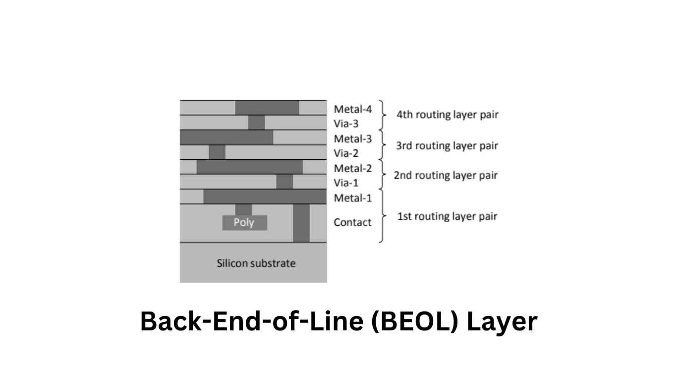
In modern semiconductor chips, the implementation of complex circuits requires multiple metallization layers. While the Front-End-of-Line (FEOL) layer designations vary between manufacturers and processes, the Back-End-of-Line (BEOL) layer designations are standardized, as depicted in Figure 1. Metal layers are typically numbered in the order of fabrication, from the bottom to the top. The layers containing through contacts between neighboring metal layers are referred to as vias, while the bottom through contacts that connect the first metal layer to the silicon surface, and consequently to the devices, are called contacts.
For each routing layer, there is a corresponding pair of two layers (Contact + Metal1 and Via[n] + Metal[n+1]) responsible for routing, as shown in Figure 1.
Materials Used for Metallization Layers
From a fabrication standpoint, the material used for metallization layers must be easy to deposit and structure while adhering well to oxide. Additionally, it should meet specific requirements for various applications:
High Electrical Conductivity: To minimize parasitic IR drops and ensure efficient electrical conductivity.
High Current-Carrying Capacity: Supporting miniaturization by carrying higher currents in smaller interconnects.
Good Silicon Contact: Facilitating the electrical connection between devices and silicon.
Good Environment Contact: Electrically connecting the entire chip as a whole.
Low Susceptibility to Corrosion: Ensuring long-term mechanical stability and avoiding degradation.
Potential for Multi-Layer Routing: Saving chip surface area and simplifying layout design.
Aluminum (Al) has been the material of choice for metallization for a significant period since it meets these requirements. By alloying aluminum with small percentages of silicon and copper (known as AlSiCu), some properties can be slightly improved.
Challenges with Aluminum and the Transition to Copper
As feature sizes shrink, aluminum’s main drawback becomes evident—it exhibits disproportionately increased parasitic resistance due to reduced interconnect cross-sectional areas. To overcome these limitations, copper has increasingly replaced aluminum in state-of-the-art processes. Copper boasts lower specific resistance than pure aluminum (approximately a factor of 2) and significantly reduces electromigration, accommodating higher current densities and enabling the design of smaller interconnects.
The adoption of copper, however, comes with its share of challenges. Copper readily contaminates surrounding materials and diffuses quickly into the surrounding oxide. It is also prone to corrosion throughout, unlike aluminum, which forms a protective surface oxide layer. To address these issues, copper requires appropriate protective coatings and necessitates the development of new structuring techniques, as it is difficult to dry etch copper.
The transition from aluminum to copper as the interconnect material typically occurs between the 350 nm and 90 nm technology nodes. Both materials can be found between these nodes. In some cases, smart power chips incorporate an extra-thick copper layer for interconnects carrying high currents, while thinner metallization layers beneath are still fabricated using aluminum.
conclusion
The choice of metallization material in semiconductor chips has significant implications for performance, power efficiency, and overall chip design. While aluminum has served as a reliable option, the switch to copper brings enhanced conductivity and reduced crosstalk, but it also introduces new challenges in fabrication and material handling. Semiconductor manufacturers carefully weigh these factors to ensure the optimal performance and reliability of their products.