
Wet Etching and Dry Etching
In semiconductor manufacturing, I see that etching is important for shaping and defining different structures on the wafer surface. You’ll often encounter two main etching methods: wet etching and dry etching. Each of these methods has its own strengths and limitations, which makes them better suited for various stages of the fabrication process.
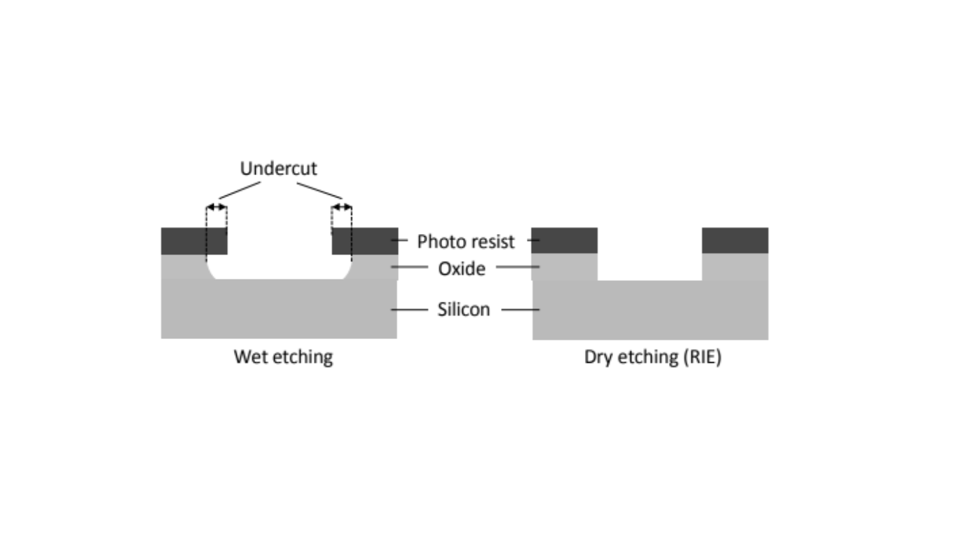
Wet Etching: Dissolving with Fluid Chemicals
In wet etching, an oxide layer is dissolved and removed using a fluid chemical etching agent. This method is simple and widely utilized, offering the advantage of adjustable etching rates. However, wet etching has a significant drawback—it is isotropic, meaning it etches in all directions. As a result, undesired lateral etching occurs beneath the photoresist layer. These lateral undercuts cause the oxide openings to be larger than the corresponding openings in the photoresist, leading to an edge shift (Above figure, left). The lateral undercutting occurs at a slightly lower etching rate compared to vertical etching, as the etching agent faces more significant saturation due to limited circulation under the photoresist. Typically, the lateral undercut can be around 80% of the etching depth.
Wet etching is not suitable for fabricating advanced semiconductor devices with typical feature sizes due to this undercutting effect. Consequently, it is primarily used in these processes to dissolve and remove entire layers.
Dry Etching: The Power of Reactive Ion Etching (RIE)
Dry etching, particularly Reactive Ion Etching (RIE), is an essential technique in semiconductor manufacturing. In this process, the etching agent is ionized and applied as a gas plasma. The ions within the plasma undergo oscillatory motion due to an electrically alternating field. This field is aligned perpendicular to the wafer surface, causing the chemically active ions to oscillate vertically and etch the material exclusively in that direction. The absence of edge shift is the main advantage of RIE (Above figure, right).
The etching effect in RIE results from a combination of physical and chemical processes. The material to be etched is bombarded with particles in a specific direction (physical effect) while simultaneously undergoing chemical etching. This combination allows for the creation of very fine structures, making the RIE process ideal for advanced semiconductor fabrication. Moreover, the resulting trenches can be much deeper than their width, enabling the production of high-aspect-ratio structures.
Conclusion
In summary, wet etching and dry etching are two fundamental techniques used in semiconductor manufacturing for different purposes. Wet etching is a straightforward method for dissolving and removing entire layers, while dry etching, particularly Reactive Ion Etching (RIE), offers precise and anisotropic etching, making it suitable for creating intricate and high-aspect-ratio structures. Understanding the strengths and limitations of each method is essential for optimizing the semiconductor fabrication process and achieving desired device characteristics.