Double patterning (DP)
Double patterning (DP) is a type of resolution enhancement method in lithography to increase the feature density or in order to achieve Higher density and better resolution, this double pattern Technology is used.
The double patterning technique is based on exposure to different reticles to offset each other, which is then followed by wafer etching process steps. Double Pattern was the key method that was applied in 28 and 22 nm half-pitch nodes by the semiconductor industry.
There are two main types of DPT, for example, Litho-etch-litho-etch (LELE) and self-aligned double patterning (SADP). LELE involves patterning the substrate twice using different masks, while SADP uses a single mask and a self-aligned process to create two patterns. There are several types of double patterning technologies ranging from double exposure (DE) to self-aligned spacer.
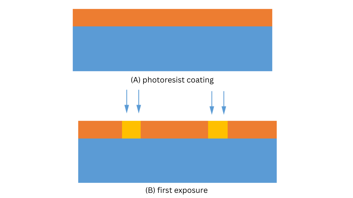
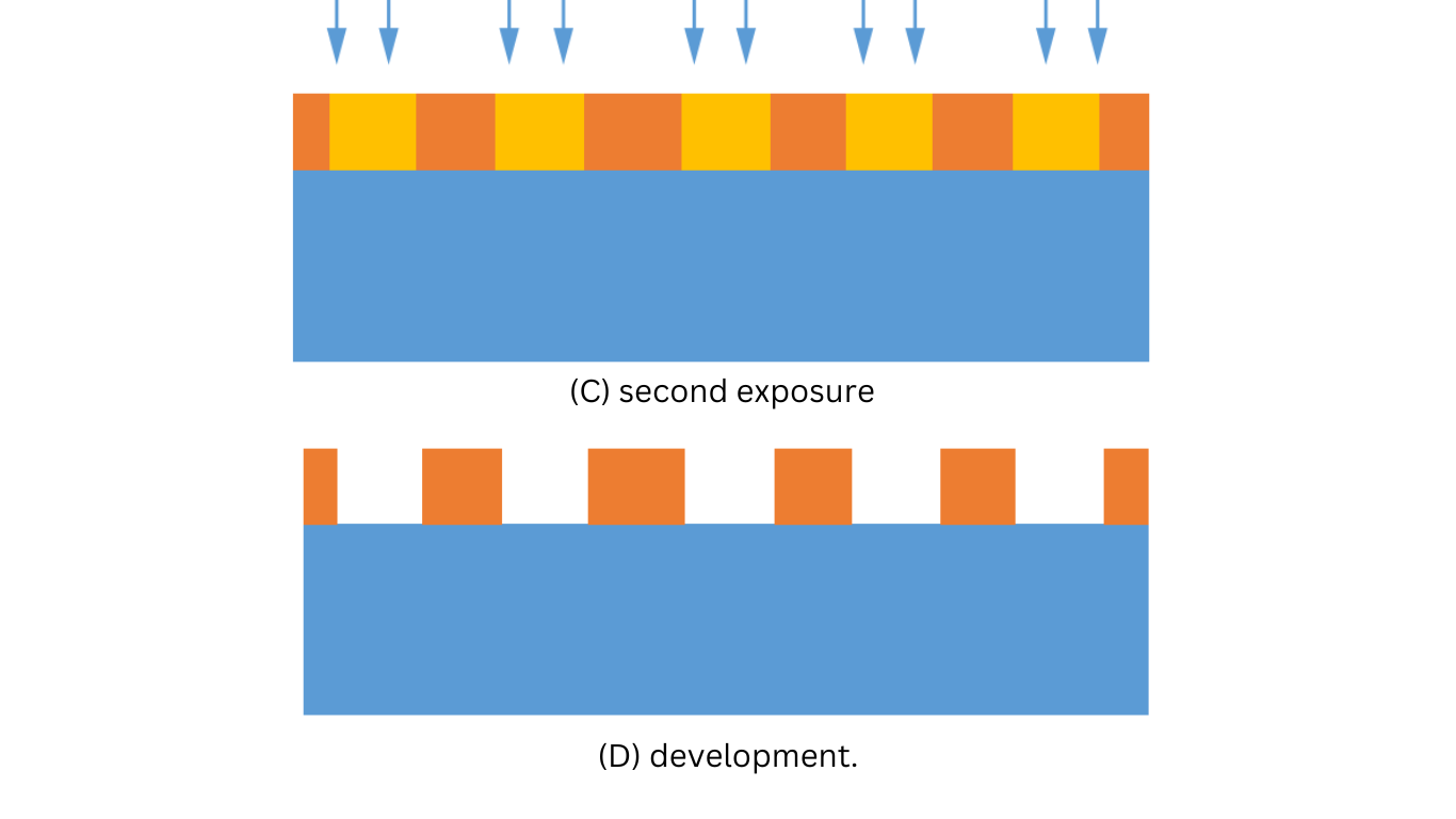
Double exposure lithography process steps
Double Exposer is two separate exposures on the same photoresist layer using two different masks in sequence. It is usually used for patterns of the same layer, which appear to be very different or have incompatible densities or spaces. Figure 1 is the description of the double-exposure lithography process.
The DE technique allows the manufacturability of the minimum spacing feature in a layout with various CDs. As long as the DE can be effectively used and is under the control of the alignment tolerance, it is a better patterning method compared to the self-aligned spacer, double expose and double etch.
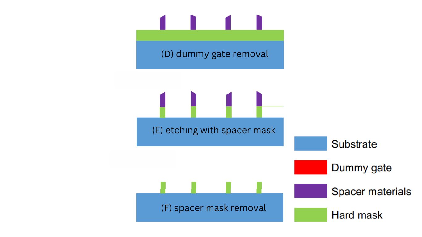
Self Align Double Patten Fabrication Process
A self-aligned spacer patterning method is used on a conformal film deposited on the patterned wafer, where spacers are initially formed and used as hard masks to etch the below layer as shown in Figure 2.
The spacer materials are commonly chosen hard mask dielectric materials (SiN and SiO2), whose etched post-pattern quality tends to be superior to the etched photoresist pattern, but it is often desirable to better control the line edge roughness.
The width of the exposed lines depends on the width of the spacer. The spacer lithography technique has most widely been applied in patterning fins for FinFETs.
Among the self-aligned spacer patterning technologies, self-aligned double patterning (SADP) and self-aligned quadruple patterning (SAQP) techniques are other important resolution enhancement methods that might be applied to the lower technology nodes
A self-aligned spacer patterning lithography process Steps are following
![]()