
How to Optimize RTL Design for Power and Performance: 7 Essential Techniques
Optimizing RTL design for power and performance is an important part of digital VLSI design. Good RTL can help reduce unnecessary switching activity, improve timing, and make better use of hardware resources before the design reaches synthesis and physical implementation[1].
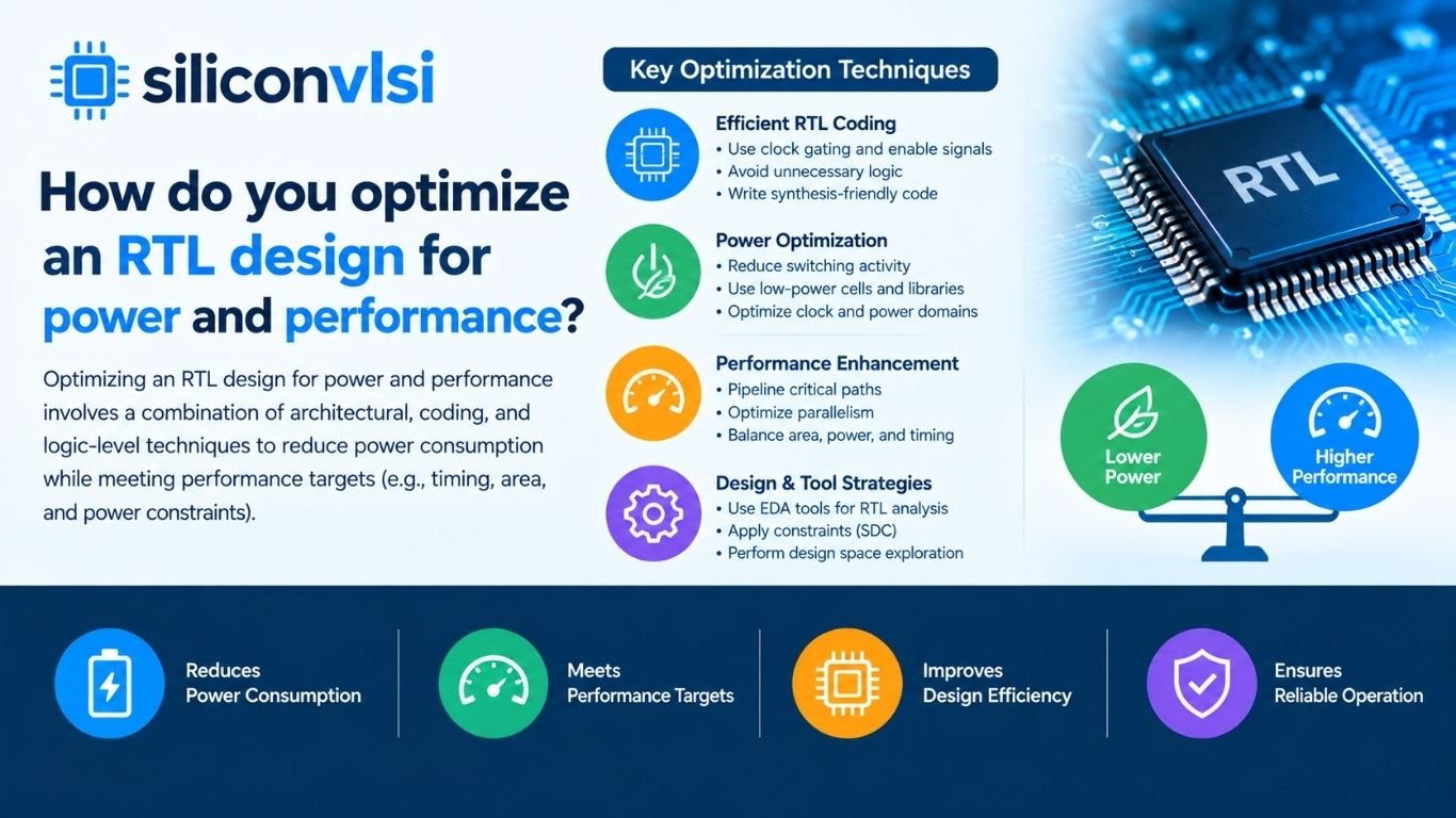
The main techniques include pipelining, clock gating, power gating, datapath optimization, control-path optimization, resource sharing, and reducing unnecessary switching activity.
Why RTL Optimization Is Important
RTL decisions can influence the final implementation in terms of:
- Power consumption
- Timing performance
- Area
- Switching activity
- Hardware utilization
- Critical-path delay
RTL optimization should therefore consider power, performance, and area together rather than optimizing one parameter in isolation.
DRC (Design Rule Check) in VLSI – Complete Guide
1. Use Pipelining to Improve Performance
Pipelining divides a long combinational path into multiple stages by inserting registers.
Without pipelining:
Input → Long Combinational Logic → Output
With pipelining:
Input → Logic → Register → Logic → Register → Output
This can reduce the amount of combinational logic that must be completed within a single clock cycle, allowing a higher operating frequency.
However, pipelining also adds registers, which can increase:
- Area
- Clock power
- Latency
Therefore, pipeline stages should be added where they provide a meaningful timing benefit.
2. Apply Clock Gating to Reduce Power
Clock networks can consume significant dynamic power because the clock switches continuously.
Clock gating prevents the clock from reaching registers when those registers do not need to change.
For example, if a register only needs to update when an enable signal is active, clock gating can reduce unnecessary clock-related switching.
A simplified concept is:
Enable = 1 → Register operates
Enable = 0 → Register remains inactive
Clock gating should be implemented using appropriate library-supported clock-gating structures rather than creating unsafe clock logic with ordinary combinational gates.
3. Use Power Gating for Leakage Reduction
Power gating disconnects selected blocks from the power supply or ground when they are not required.
This can reduce leakage power during inactive periods.
A typical power-gated design may contain:
Power Supply → Header Switch → Logic Block → Ground
Power gating is particularly useful for blocks that can remain inactive for significant periods.
However, it introduces additional considerations such as:
- Wake-up time
- State retention
- Power-domain control
- Isolation
- Inrush current
4. Optimize the Datapath
The datapath contains hardware used to process and transfer data, such as:
- Adders
- Multipliers
- Multiplexers
- Comparators
- Registers
- Shifters
Optimizing the datapath can improve both power and performance.
For example, unnecessary arithmetic operations can be eliminated, and hardware resources can sometimes be reused when operations do not occur simultaneously.
Reducing unnecessary logic can decrease both switching activity and circuit area.
LVS (Layout Versus Schematic) in VLSI: Complete Guide, Flow, Errors and Interview Questions
5. Optimize the Control Path
The control path determines how and when different parts of the design operate.
Poorly structured control logic can create unnecessary transitions and additional combinational delay.
Useful techniques include:
- Simplifying Boolean logic.
- Reducing unnecessary state transitions.
- Optimizing finite-state machines.
- Avoiding unnecessary control signals.
- Ensuring inactive blocks do not switch unnecessarily.
A simpler control path can make the design easier to verify and may also improve timing and power characteristics.
6. Reduce Unnecessary Switching Activity
Dynamic power is strongly related to switching activity.
A commonly used CMOS dynamic-power relationship is:
Pdynamic ≈ α × C × VDD² × f
where:
- α = switching activity
- C = effective capacitance
- VDD = supply voltage
- f = clock frequency
At the RTL level, designers can reduce unnecessary switching by avoiding needless data transitions and preventing inactive logic from continuously evaluating changing inputs.
Techniques such as operand isolation can prevent unnecessary activity in datapath blocks when their results are not required.
7. Optimize Resource Sharing
Multiple operations may sometimes use the same hardware resource rather than requiring separate copies.
For example, two operations that never occur at the same time might share an arithmetic unit through appropriate control and multiplexing.
This can reduce:
- Area
- Leakage power
- Potential switching in duplicated logic
However, excessive resource sharing can introduce additional multiplexers and longer paths. Therefore, the timing impact should be checked before applying it.
Power vs Performance Trade-Off
RTL optimization often involves trade-offs.
| Technique | Power Impact | Performance Impact | Main Consideration |
|---|---|---|---|
| Pipelining | Can increase clock power | Can improve frequency | Adds registers |
| Clock gating | Reduces dynamic power | Usually small control overhead | Clock implementation |
| Power gating | Reduces leakage | Adds wake-up overhead | Power-domain design |
| Datapath optimization | Can reduce power | Can improve timing | Functionality |
| Control optimization | Can reduce switching | Can improve logic delay | FSM complexity |
| Operand isolation | Reduces unnecessary switching | May add control logic | Isolation overhead |
| Resource sharing | Can reduce area/power | May increase delay | Multiplexer overhead |
RTL Optimization Flow
A practical optimization process can be viewed as:
RTL Design → Functional Verification → Synthesis → Timing/Power Analysis → Identify Critical Areas → RTL Optimization → Re-verify
The important point is that RTL optimization should be based on actual analysis rather than simply applying every optimization technique.
For example, if timing analysis identifies a critical datapath, pipelining or logic restructuring may be considered. If power analysis identifies excessive switching in an inactive block, clock gating or operand isolation may be more appropriate.
Common RTL Optimization Mistakes
Some common mistakes include:
- Adding pipeline stages without considering latency.
- Using incorrect clock-gating structures.
- Sharing resources without checking timing.
- Optimizing area while creating a timing violation.
- Reducing switching in one block while increasing switching elsewhere.
- Making RTL unnecessarily complex.
- Changing RTL without re-running functional verification.
Frequently Asked Questions
What is RTL optimization?
RTL optimization is the process of modifying hardware descriptions to improve characteristics such as power, performance, and area while maintaining the required functionality.
How does pipelining improve performance?
Pipelining divides a long combinational path into smaller stages, allowing the design to operate at a higher clock frequency when the resulting pipeline stages meet timing requirements.
How does clock gating reduce power?
Clock gating prevents unnecessary clock transitions from reaching inactive sequential logic, reducing dynamic power associated with clock and register switching.
What is the difference between clock gating and power gating?
Clock gating primarily reduces dynamic switching activity, while power gating disconnects or limits power to an inactive block and is mainly used to reduce leakage power.
Can RTL optimization reduce both power and improve performance?
Yes, some optimizations can benefit both, but there are often trade-offs. An optimization that improves timing may increase area or power, while an optimization that reduces power may introduce additional delay.
Conclusion
RTL design optimization for power and performance requires careful control of switching activity, timing, and hardware resources.
Techniques such as pipelining, clock gating, power gating, datapath optimization, control-path optimization, operand isolation, and resource sharing can help improve the implementation.
The most effective approach is to measure the design, identify the actual power or timing bottleneck, apply an appropriate RTL change, and then verify the resulting implementation.
References
- E. Macii, “RTL power estimation and optimization”, in Proceedings of the 17th symposium on Integrated circuits and system design, New York, NY, USA: ACM, Sep. 2004, pp. 1–1. doi: 10.1145/1016568.1016575.