
Understanding minority charge injection
A p-n junction diode is a two-terminal or two-electrode semiconductor device, which allows the electric current in only one direction while blocking the electric current in the opposite or reverses direction. and If the diode is forward-biased, it allows the electric current to flow. if the diode is reverse-biased, it blocks the electric current flow. A p-N junction semiconductor diode is also called a p-n junction semiconductor device.
Working of P-N junction Diode
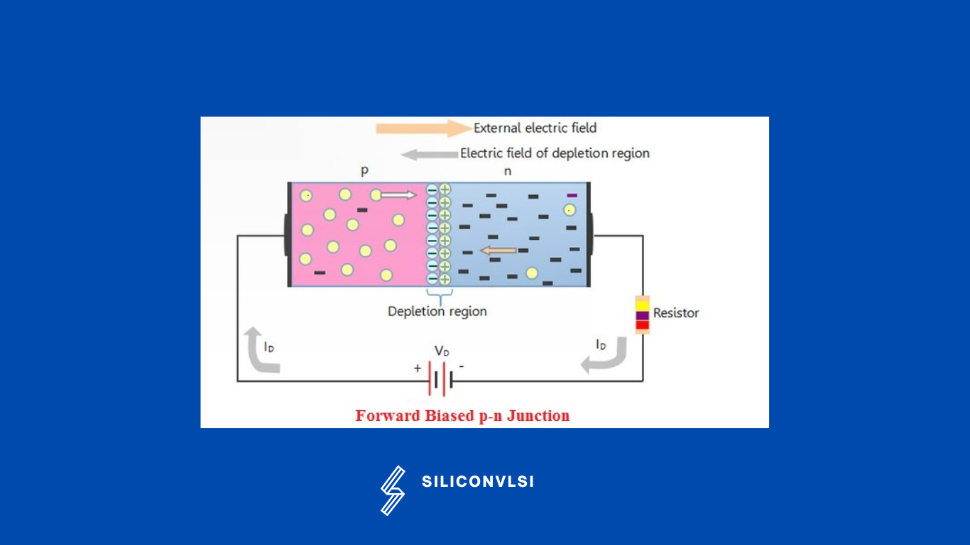
A pn junction has two sides, a-holes are in the p side, and an electron-are in n side. On the p side, holes are the majority carriers and electrons are minority carriers and on the n side, electrons are the majority carriers and holes are minority carriers. When we applied a positive bias to the junction, which means that the p side is attached to the positive terminal of a battery and the n side is attached to the negative side, the current will flow. The holes are attracted to the negative terminal and the electrons to the positive terminal so that the holes from the p side are “injected” into the n side and vice-versa. The two types of carriers are injected into the side in which they are minority carriers. This is also called minority carrier injection.
What is the depletion region in the PN junction?
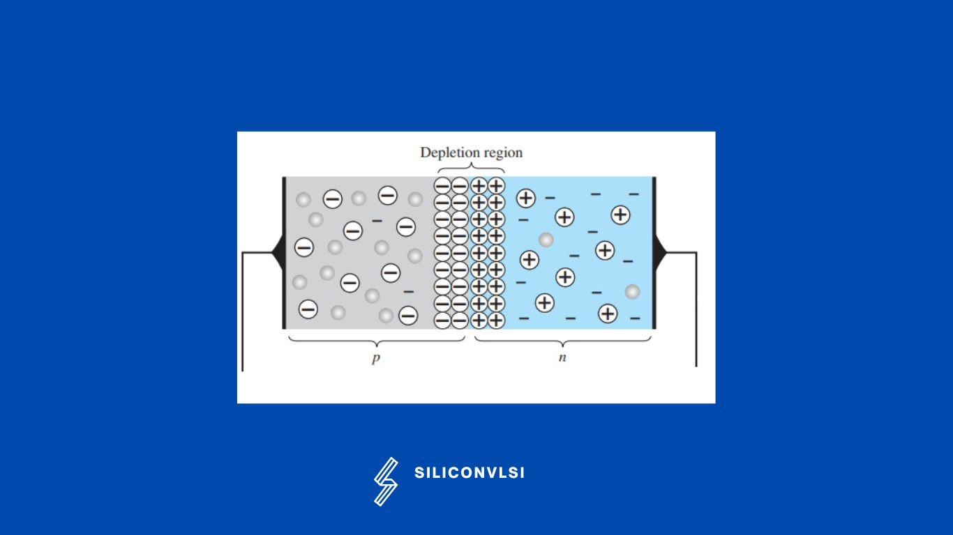
The depletion region is a region in a P-N junction diode where no mobile charge carriers are present. The depletion layer acts like a barrier that opposes the flow of electrons from the n-side and holes from the p-side. It is also called the Depletion layer
What are Drift and Diffusion current
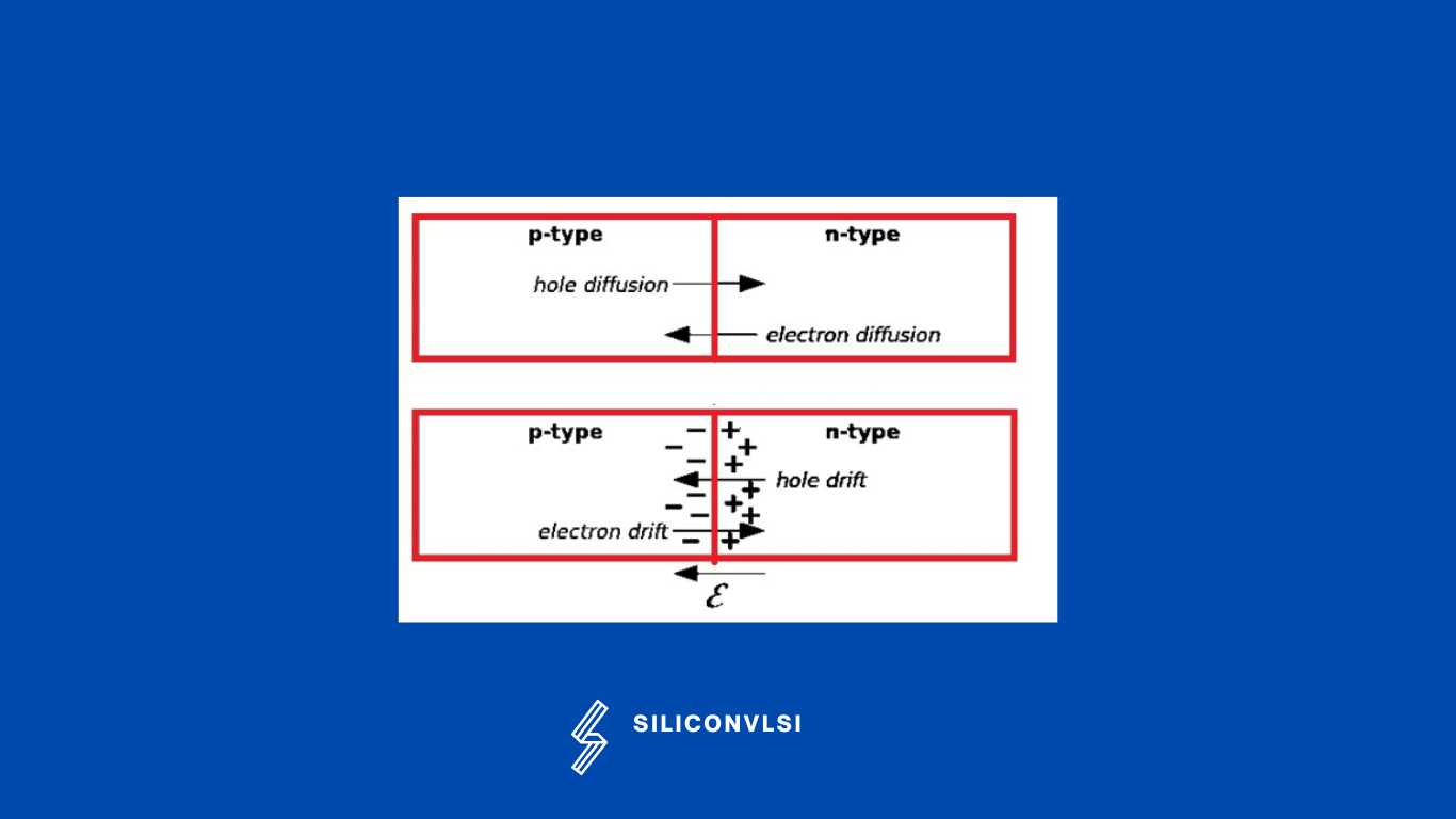
Diffusion Current
The diffusion current can be defined as the flow of charge carriers within a semiconductor that travels from a higher concentration region to a lower concentration region. The direction of this current mainly depends on the charge within the concentrations of the carrier.
Drift current
Drift current can be defined as the charge carrier’s moves in a semiconductor because of the electric field. The direction of this current mainly depends on the polarity of the applied electric field.
What is Equilibrium in pn junction diode?
When there is a balance between drift and diffusion for electrons and holes its called Equilibrium, or in equilibrium, the p-n junction has the same number of majority and minority carriers moving in opposite directions
Jdrift = J diff
What is the Recombination Process in Semiconductors?
When an electron loses energy and falls into the valance band, it gets neutralized by a hole that absorbs its energy. This process is called the recombination process and the energy of recombination will emerge as a photon.
What is the basic principle of carrier injection?
Hot carrier injection in MOSFETs happens when a carrier from the silicon channel is injected into the gate oxide. For this process to occur, a carrier must possess sufficient kinetic energy to reach the conduction or valence band in the oxide. Specifically, the required energy amounts for an electron and a hole are 3.2 and 4.6 electron volts (eV), respectively.