Close Menu
  • Analog Design
    • Latest Analog Layout Interview Questions (2025)
  • Digital Design
    • Digital Electronics Interview Question(2025)
    • Top VLSI Interview Questions
  • Physical Design
    • Physical Design Interview Questions for VLSI Engineers
  • Verilog
    • Verilog Interview Questions(2024)
  • Forum
Facebook Instagram YouTube LinkedIn WhatsApp
SiliconvlsiSiliconvlsi
Forum Questions Register in Forum Login in Forum
Facebook Instagram YouTube LinkedIn WhatsApp
  • Analog Design
    • Latest Analog Layout Interview Questions (2025)
  • Digital Design
    • Digital Electronics Interview Question(2025)
    • Top VLSI Interview Questions
  • Physical Design
    • Physical Design Interview Questions for VLSI Engineers
  • Verilog
    • Verilog Interview Questions(2024)
  • Forum
SiliconvlsiSiliconvlsi
Home»VLSI Design»Intrinsic semiconductor: Fundamentals of Semiconductor physics
VLSI Design

Intrinsic semiconductor: Fundamentals of Semiconductor physics

siliconvlsiBy siliconvlsiApril 5, 2022Updated:June 4, 2024No Comments2 Mins Read
Facebook Pinterest LinkedIn Email WhatsApp
Share
Facebook Twitter LinkedIn Pinterest Email

Intrinsic semiconductor: Fundamentals of Semiconductor physics

Intrinsic Semiconductor comes in between conductor and insulators. It is e made from the purest form of semiconductor material. The best examples of Intrinsic Semiconductor are Silicon & Germanium


 Silicon and Germanium Electronic Configuration
Silicon 1s2 2s22p6 3s2 3p2
Germanium 1s2 2s2 2p6 3s2 3p6 4s2 3d10 4p2


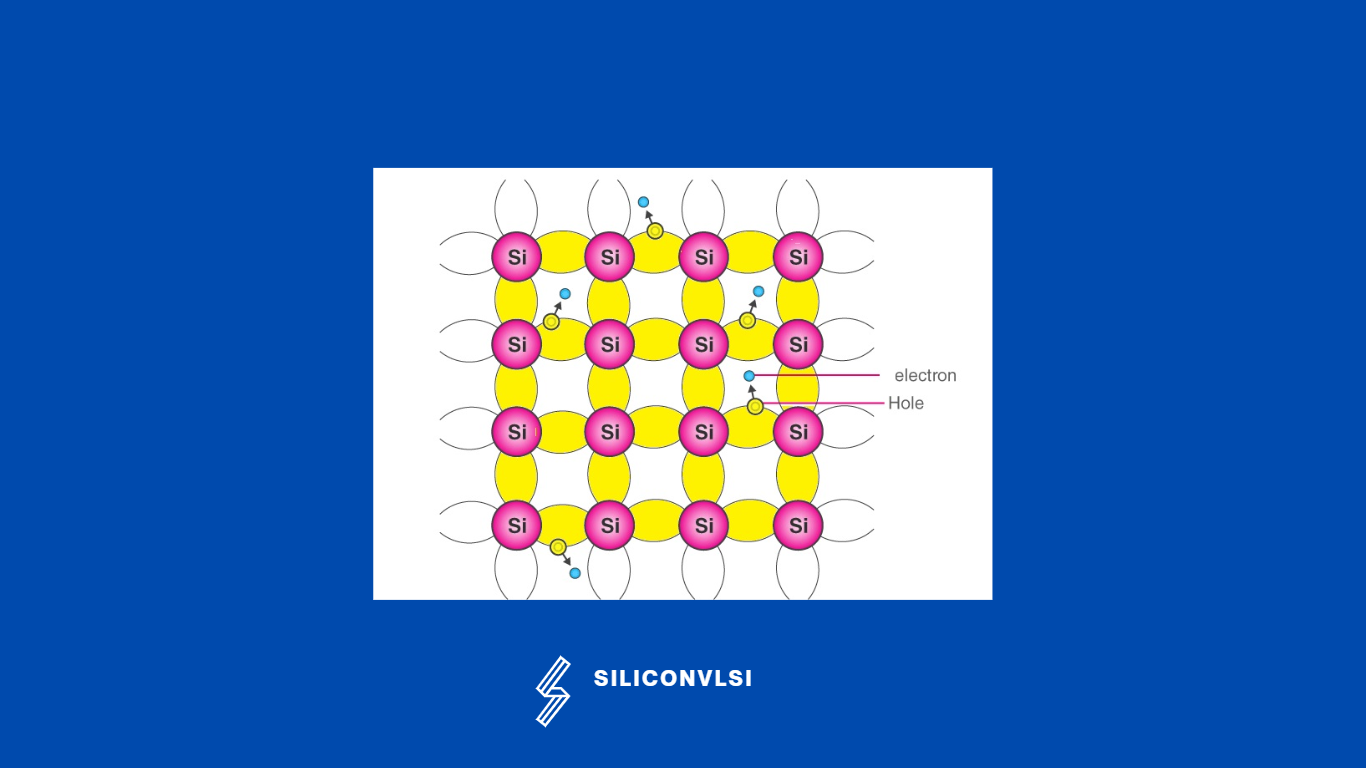
  • An intrinsic semiconductor, such as pure silicon has an equal number of electrons and holes.
  • In a P-type semiconductor, holes are the majority charge carriers electrons called minority carriers.
  • In N-type semiconductors, electrons are the majority charge carriers and holes are the minority carriers
Intrinsic Semiconductor

Use of Intrinsic Semiconductor

An intrinsic semiconductor is also called an undoped semiconductor. Silicon and germanium are the most common examples of intrinsic semiconductors. Both these semiconductors are most frequently used in the manufacturing of transistors, diodes, and other electronic components. 

What is Electron current and Hole current?

Electron current: The current which flows in a circuit due to the flow of electrons, is the electron current. The direction of the electron is negative to positive.

Hole current: The current which flows in a circuit due to the flow of holes, is the hole current. The direction of the hole is positive to negative.


Electron and Hole current

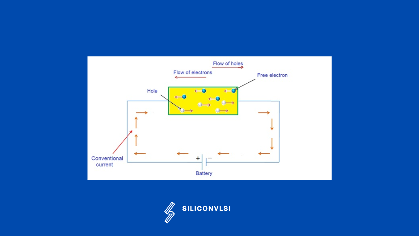
In other words, we can say that a Current that is caused by electron motion is called electron current, and a current that is caused by hole motion is called hole current. An electron is a negative charge carrier whereas a hole is a positive charge carrier.


  • N Type Semiconductor
  • P Type Semiconductor
  • Intrinsic Semiconductor
  • Extrinsic Semiconductor
  • Difference Between Donor and Acceptor Impurities
  • Difference Between p-Type and n-Type Semiconductor
  • Electron Hole Pairs Generation and Recombination


Share. Facebook Twitter Pinterest LinkedIn Tumblr Email

Related Posts

How Shielding Avoids Crosstalk Problem? What Exactly Happens There?

September 22, 2024

Navigating the Challenges of Gate Dielectric Scaling in MOS Transistors

August 1, 2024

Challenges in Modern SoC Design Verification

April 20, 2024
Leave A Reply Cancel Reply

Facebook X (Twitter) Instagram Pinterest Vimeo YouTube
  • About Us
  • Contact Us
  • Privacy Policy
© 2025 Siliconvlsi.

Type above and press Enter to search. Press Esc to cancel.