
Heat and Mechanical Stress in Layout
In semiconductor device design, various factors like heat distribution and mechanical stress can affect the electrical properties of devices. When these gradients are known, specific optimization strategies can be employed to achieve better device matching. Here’s how to address heat distribution and mechanical stress:
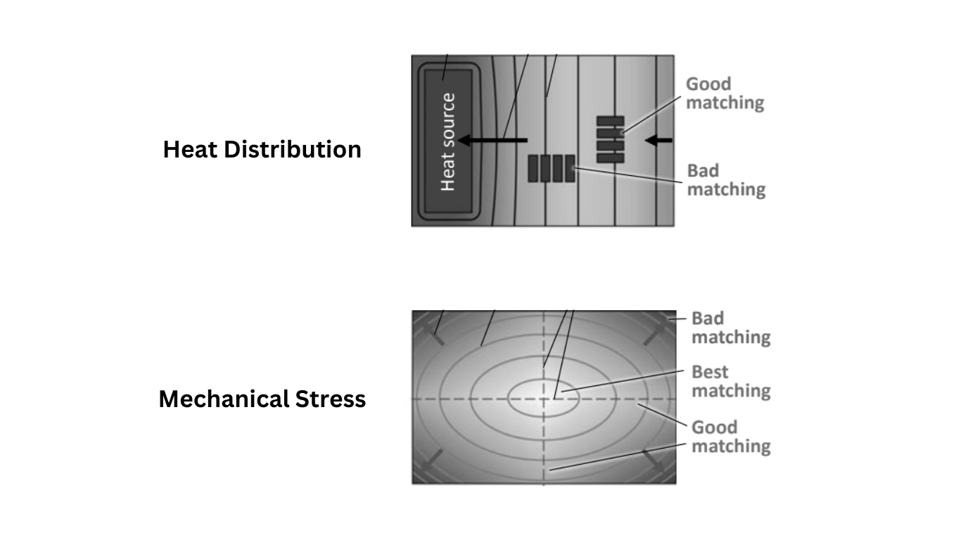
Heat Distribution on the Chip
Integrated circuits generate significant thermal losses due to high power densities. This heat is not evenly distributed across the chip.
Power transistors, such as DMOS-FETs, can be major heat sources, creating temperature differences on the chip.
The matching process is primarily concerned with temperature differences rather than absolute temperatures.
Rule of Thumb for Heat-Related Matching
Place matching devices along isotherms, which are lines of constant temperature.
Isotherms help minimize temperature-related mismatches.
This rule applies to common centroid layouts as well.
Mechanical Stress
During chip packaging, the injected mold mass exerts pressure on the die, leading to permanent deformation of the silicon crystal.
This mechanical stress can significantly impact the mobility of charge carriers and, consequently, the electrical properties of devices.
The exact regions on the chip affected by mechanical stress depend on the crystal lattice alignment.
Rule of Thumb for Managing Mechanical Stress
Avoid chip regions with high-stress gradients, especially when tight matching requirements are essential.
The chip’s center is an ideal location for achieving good matching results, as stress levels are typically lower.
Along the two centerlines of the chip, where stress gradients are moderate, good matching results can also be attained.
In summary, when known gradients, such as heat distribution and mechanical stress, impact semiconductor devices, it’s possible to optimize device placement to minimize mismatches. Placing matching devices along isotherms for temperature-related mismatches and avoiding high-stress gradient regions within the chip are effective strategies for achieving better device matching and ensuring reliable circuit performance.