
Epi Substrates and Retrograde Wells in Improving Latch-Up Stability in CMOS Circuits
Epi substrates have a weakly doped epitactic layer at the surface, while retrograde wells use a high-energy implanter to create a highly doped region at the bottom of the well. Let’s understand it in detail
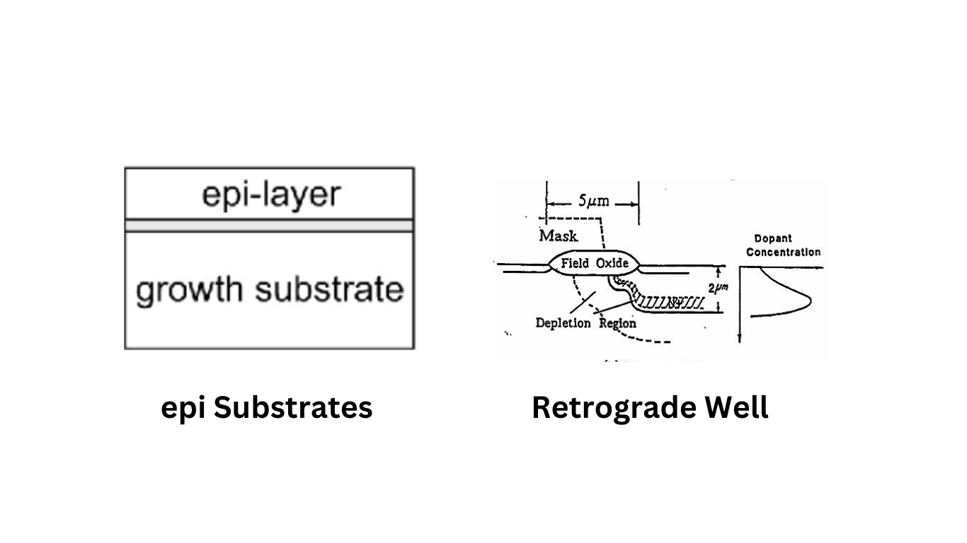
Epi Substrates
Epi substrates, short for epitaxial substrates, are a common technique used in CMOS circuit design to enhance latch-up stability. Here’s how they work:
- Surface Epitaxy: In an epi substrate, a weakly doped epitaxial layer is grown on top of the bulk silicon substrate. This epitaxial layer has lower dopant concentrations compared to the bulk silicon.
- Reduced Parasitic Thyristor Sensitivity: The key advantage of epi substrates is that they reduce the sensitivity of the parasitic thyristor to latch-up conditions. The presence of the lightly doped epitaxial layer alters the electrical characteristics near the surface.
- Weakened Parasitic Transistors: Due to the lower dopant concentrations in the epitaxial layer, the parasitic NPN and PNP transistors within the CMOS structure are weakened. Specifically, the lower doping reduces the gain of these parasitic transistors, making it less likely for them to turn on unintentionally.
- Latch-Up Prevention: By weakening these parasitic transistors, epi substrates effectively prevent latch-up events. They provide an additional layer of protection against the conditions that could trigger latch-up in CMOS circuits.
Retrograde Wells
Retrograde wells are another technique used to enhance latch-up stability in CMOS circuits. Here’s how they work:
- High-Energy Implantation: In the case of retrograde wells, a high-energy ion implantation process is employed. This process introduces dopant atoms deep into the silicon substrate.
- Highly Doped Bottom Region: The key feature of retrograde wells is that they create a highly doped region at the bottom of the well. This region has a much higher dopant concentration compared to the surrounding silicon.
- Reduced Collector Resistance: The highly doped region at the well’s bottom significantly reduces the collector resistance of the parasitic NPN transistor. This reduction in resistance makes it less likely for the NPN transistor to turn on unintentionally.
- Latch-Up Prevention: Similar to epi substrates, retrograde wells help prevent latch-up by reducing the susceptibility of the parasitic transistors within the CMOS structure to latch-up conditions.
In summary, both epi substrates and retrograde wells are techniques used to modify the silicon substrate’s doping profile in CMOS circuits, specifically to reduce the sensitivity of parasitic transistors to latch-up. Epi substrates achieve this by growing a weakly doped epitaxial layer on the surface, while retrograde wells create a highly doped region at the well’s bottom. These modifications strengthen latch-up prevention mechanisms, improving the overall latch-up stability of CMOS circuits and ensuring their reliable operation.