Close Menu
  • Analog Design
    • Latest Analog Layout Interview Questions (2025)
  • Digital Design
    • Digital Electronics Interview Question(2025)
    • Top VLSI Interview Questions
  • Physical Design
    • Physical Design Interview Questions for VLSI Engineers
  • Verilog
    • Verilog Interview Questions(2024)
  • Forum
Facebook Instagram YouTube LinkedIn WhatsApp
SiliconvlsiSiliconvlsi
Forum Questions Register in Forum Login in Forum
Facebook Instagram YouTube LinkedIn WhatsApp
  • Analog Design
    • Latest Analog Layout Interview Questions (2025)
  • Digital Design
    • Digital Electronics Interview Question(2025)
    • Top VLSI Interview Questions
  • Physical Design
    • Physical Design Interview Questions for VLSI Engineers
  • Verilog
    • Verilog Interview Questions(2024)
  • Forum
SiliconvlsiSiliconvlsi
Home»VLSI Design»Latch-up in CMOS circuits
VLSI Design

Latch-up in CMOS circuits

siliconvlsiBy siliconvlsiApril 6, 2022Updated:June 4, 2024No Comments2 Mins Read
Facebook Pinterest LinkedIn Email WhatsApp
Share
Facebook Twitter LinkedIn Pinterest Email

Latch-up in CMOS circuits

Latch-Up is a phenomenon where a low impedance path is created between a supply pin and ground due to unwanted noise. It is also called when minority carriers are injected into the substrate of a well.
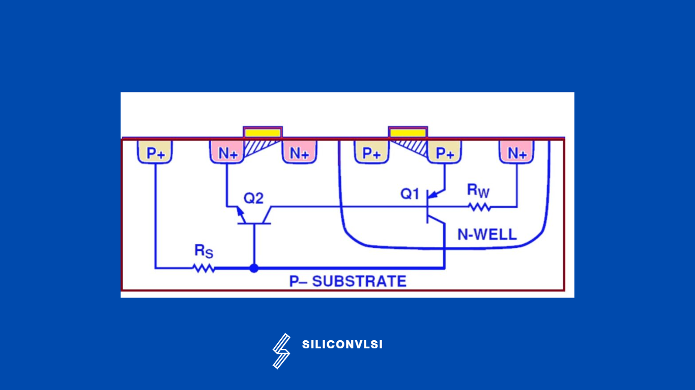
Latch-up Mechanism

The parasitic BJTs in the CMOS inverter structure form a positive feedback loop and are well known that the large collector current of a BJT is driven by a much smaller base current. Now, if for some reason a collector current flows in one of the BJTs, it will be fed into the base of the other BJT. This generates an even greater collector current in the latter BJT which is then fed into the former BJT. When the BJTs become locked in this runaway positive feedback process, they are said to be latched. In this latch-up condition, a low-impedance path is created between the VDD & VSS

What is Latch-up?
What is Latch-up?

Latch-up Causes

  • Noise
  • ionizing radiation
  • If we put NMOS & PMOS closer 
  • Sudden changes in supply voltage
  • Due to Minority charge carrier injection
  • An electrostatic discharge (ESD) event can trigger the parasitic SCR

Latch-up Prevention Techniques

  • Keep supply voltage below the maximum voltage.
  • Keep NMOS & PMOS as far as possible.
  • Use oxide trenches and buried oxide layers to isolate NMOS and PMOS devices.
  • keep a Guard ring for the analog device and tap/bulk for the digital logic device.
  • Use halo dopping 

Why is a PMOS connected to a VDD and NMOS connected to the ground?

Because, to prevent latch-up in CMOS, the body-source and body-drain diodes should not be forward-biased. For example, the body terminal should be at the same or lesser voltage than the source terminal (for an NMOS) & for PMOS.

Share. Facebook Twitter Pinterest LinkedIn Tumblr Email

Related Posts

How Shielding Avoids Crosstalk Problem? What Exactly Happens There?

September 22, 2024

Navigating the Challenges of Gate Dielectric Scaling in MOS Transistors

August 1, 2024

Challenges in Modern SoC Design Verification

April 20, 2024
Leave A Reply Cancel Reply

Facebook X (Twitter) Instagram Pinterest Vimeo YouTube
  • About Us
  • Contact Us
  • Privacy Policy
© 2025 Siliconvlsi.

Type above and press Enter to search. Press Esc to cancel.