
What is Logic Gates
A logic gate is a device that acts as a building block for digital circuits. Logic functions provide ways to combine different digital signals – or signals that can only take one of two possible levels: low level 0 and high level 1 – based on the laws of Boolean algebra. These laws are applied using logic gates, which can be classified according to the number of available inputs.
An electrical circuit is comparable to each logic gate. An electrical logic gate is very similar to an electronic logic gate, but they are very different. It uses less electric power and is much faster, smaller, and more compact. On the basis of fundamental Boolean operations, logic gates can be utilized to integrate digital signals.
NOT gate
The NOT function provides the complementary state to a given variable. The function is represented by a bar placed above the input variable and implemented by a NOT gate or logic inverter. #

The logic level of the output variable is obtained by taking the complement of the input variable, as shown in the truth table given in Table. Thus, if the input is at logic level 0, the output will be at logic level 1, and vice versa.
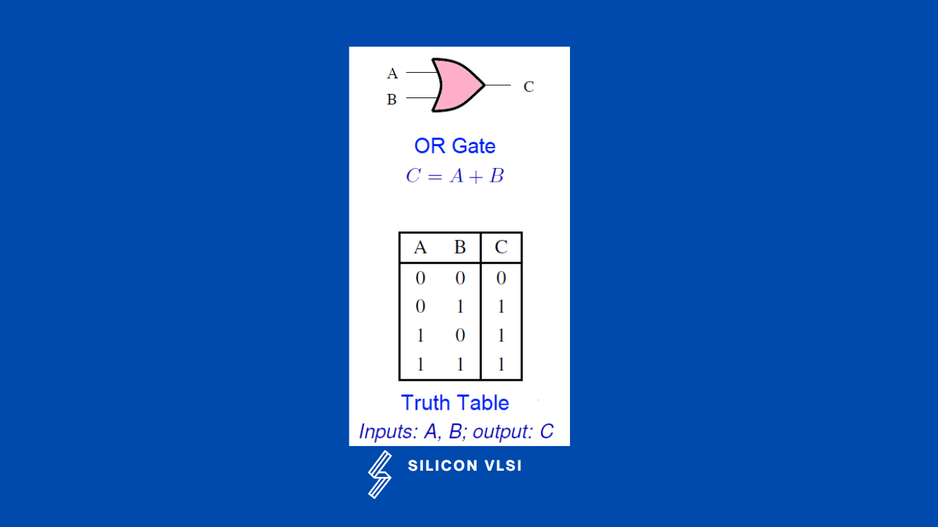
OR gate
AND gate
AND gate also has two or more input signals same as that of the OR gate, and the output is single. The gate has a high output only when all the input signals are high otherwise the output signal is low. The AND function, which is also called logic product, is represented by a dot (·).
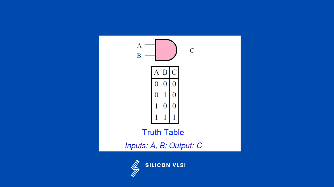
The AND gate can have two inputs, as illustrated in the above Figure, the output variable takes the high logic level (or the value 1) if and only if the input variables are both at the high logic level (or the value 1). In all other cases, the output is set to the low logic level (or the value 0). The table shows the truth table for the AND gate. #
XOR gate
Ex OR gate is the Exclusive OR gate. This is not frequently used as an inclusive OR gate, which is nothing but the regular OR gate. XOR gate has its own significance. The XOR (exclusive OR) function is represented by a plus within a circle (⊕). #
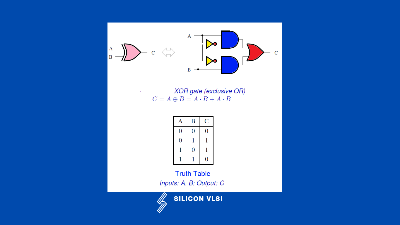
The above Figure depicts the symbolic representation of an XOR gate having two inputs. According to the truth table shown in the above table, the output takes either logic level 1, when only one of the inputs is at logic level 1, or logic level 0 when both inputs are either at logic level 0 or at logic level 1.