
What is Clock Skew?
When designing synchronous circuits, you may encounter an important phenomenon called clock skew. It happens when the clock signal from the clock circuit reaches different components at different times. In this discussion, we’ll look into the causes and effects of clock skew, highlighting both its negative and positive impacts. Together, we’ll also explore practical strategies to minimize clock skew and optimize circuit performance through effective clock skew management.
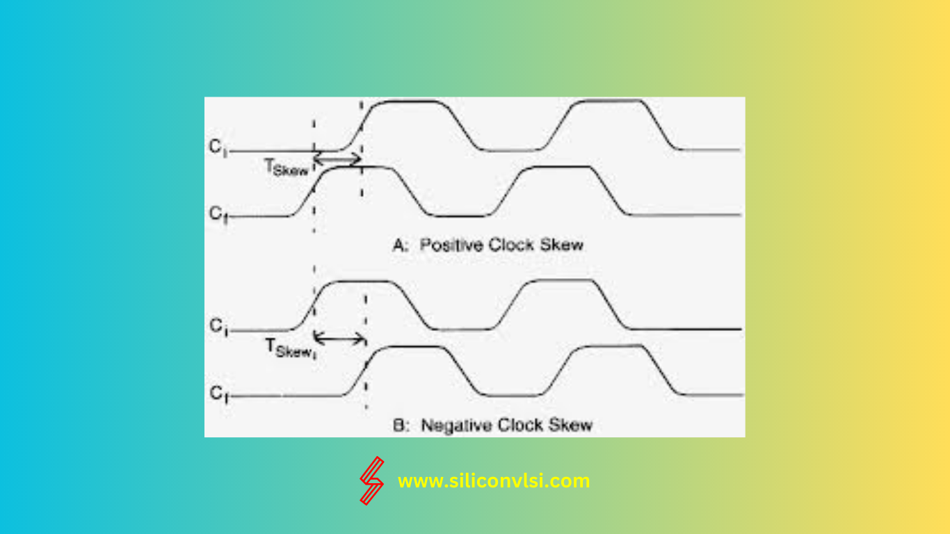
Understanding Clock Skew
Clock skew can be attributed to two primary factors. The first factor is material flaws, which can cause the signal to propagate faster or slower than anticipated. The second factor is distance. As the signal traverses the entire circuit, it is prone to arriving at different points within the circuit at different times. The magnitude of the clock skew may vary depending on the size of the circuit.
Negative Impact of Clock Skew Clock skew can have adverse effects on circuit operation, particularly in relation to data integrity. Consider a scenario where a logic path extends from a source flip-flop to a destination flip-flop. If the destination flip-flop receives the clock tick later than the source flip-flop and the logic path delay is sufficiently short, the data signal might reach the destination flip-flop before the clock tick, resulting in the corruption of the previous data that should have been clocked through. This situation is referred to as a hold violation, as the previous data is not retained long enough at the destination flip-flop for proper clocking.
On the other hand, if the destination flip-flop receives the clock tick earlier than the source flip-flop, the data signal has less time to reach the destination flip-flop before the next clock tick. Failure to do so can lead to a setup violation, where the new data is not adequately established and stable before the subsequent clock tick. While both hold and setup violations are problematic, a hold violation is considered more critical as increasing the clock period cannot resolve it.
Leveraging Clock Skew for Circuit Optimization Interestingly, when harnessed appropriately, clock skew can also bring benefits to a circuit. It can be intentionally introduced to lower the clock period required for the circuit to operate correctly. Additionally, it can increase the setup or hold safety margins, contributing to enhanced circuit stability. Determining the optimal set of clock delays is achieved through a linear program that incorporates setup and holds constraints for each logic path. In this linear program, zero clock skew merely represents a feasible point on the optimization landscape.
Minimizing Clock Skew: Effective Strategies
To minimize clock skew and ensure optimal circuit performance, several strategies can be employed:
Proper Routing of Clock Signals: Implementing a well-designed clock distribution tree is important. By carefully routing the clock signals, it is possible to ensure that all clock inputs reach their destinations simultaneously, minimizing skew.
Variable Delay Buffers: The inclusion of variable delay buffers can also mitigate clock skew. By strategically placing these buffers, it is possible to synchronize the arrival of clock signals, eliminating variations in arrival times and reducing skew.
Conclusion Clock skew poses both challenges and opportunities in synchronous circuit design. While it can detrimentally affect data integrity, it can also be leveraged to optimize circuit performance. By implementing effective clock skew management techniques such as proper signal routing and variable delay buffers, circuit designers can mitigate skew-related issues and unlock the full potential of their designs. With careful consideration and meticulous implementation, clock skew can be harnessed as a powerful tool for enhancing circuit functionality and performance.