
MOSFET
When a positive voltage (VGS) is applied to the gate of a MOSFET, several key processes occur:
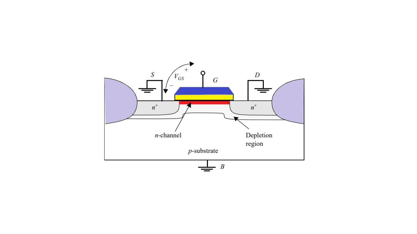
Depletion Region Formation: Initially, a positive charge accumulates on the gate electrode, creating a negative charge on the substrate side. This leads to the repulsion of mobile holes in the substrate, resulting in the formation of a depletion region beneath the gate. This depletion region is conceptually similar to what happens in a pn-junction diode, and its width and space charge per unit area can be described using mathematical expressions akin to those for diode depletion regions.
Strong Inversion: As the gate voltage continues to rise, the potential at the silicon surface eventually reaches a critical value, causing the semiconductor surface to invert into n-type material. This phenomenon, known as “strong inversion,” occurs at a voltage approximately twice the Fermi Potential (fF). Typically, for p-type silicon substrates, fF is around -0.3 V.
Inversion Layer Formation: Further increases in gate voltage result in more electrons accumulating in the inversion layer under the gate oxide. These electrons are drawn from the heavily doped n+ source region, creating a continuous n-type channel between the source and drain. The conductivity of this channel is controlled by the gate-source voltage.
In the presence of an inversion layer, the charge stored in the depletion region is fixed, and the threshold voltage (VT) is reached. The threshold voltage is a function of various factors, including the difference in work function between the gate and substrate materials, oxide thickness, Fermi voltage, impurity charges at the channel-gate oxide interface, and ion implantation for threshold adjustment.
What happens to the resistance between the drain and source terminals of a MOSFET when the gate-source voltage (VGS) is set to 0 and all terminals are grounded?
When VGS is set to 0 and all terminals are grounded, both back-to-back pn-junctions (substrate-source and substrate-drain) are considered off, resulting in an extremely high resistance between the drain and source terminals.
How does the application of a positive voltage to the gate affect the semiconductor material beneath it?
Applying a positive voltage to the gate causes a positive charge to accumulate on the gate electrode and a negative charge on the substrate side. This leads to the formation of a depletion region beneath the gate, similar to what occurs in a pn-junction diode.
What is the significance of the term “strong inversion” in the operation of a MOSFET?
“Strong inversion” marks the point at which the semiconductor surface beneath the gate inverts to n-type material. This point determines the onset of the MOSFET’s operation as a conducting channel is formed between the source and drain regions.
How is the threshold voltage (VT) defined for a MOSFET, and what factors influence its value?
The threshold voltage (VT) is the gate-source voltage at which strong inversion occurs. It depends on various factors, including the difference in work function between the gate and substrate material, oxide thickness, Fermi voltage, charge of impurities at the channel-gate oxide interface, and ion implantation dosage for threshold adjustment.
What is the role of the body-effect coefficient (g or gamma) in MOSFET operation?
The body-effect coefficient (gamma) expresses the impact of changes in the source-bulk voltage (VSB) on the threshold voltage (VT). It helps account for the influence of VSB on VT. The threshold voltage VT0 is an empirical parameter representing the threshold voltage for VSB = 0, primarily determined by the manufacturing process. VT for different VSB values can be determined using VT0 and gamma