
Steps Involved in Small-Signal Analysis of MOSFET
When we talk about small signal MOSFETs, we’re referring to a portfolio that includes small signal N-channel MOSFETs and small signal P-channel MOSFETs, also known as small signal PMOS and NMOS. These MOSFETs offer a wide range of drain-source on resistance (R(DS)on) values and voltage classes.
When to Use a Small-Signal Model?
You should use small signal analysis when you want to ignore the non-linear behavior of the transistor and instead focus on variations in the voltage/current values from their bias conditions. For example, this is useful when you’re looking at how a microphone amplifier responds to a small audio signal.
Amplifying Small Signals with MOSFETs
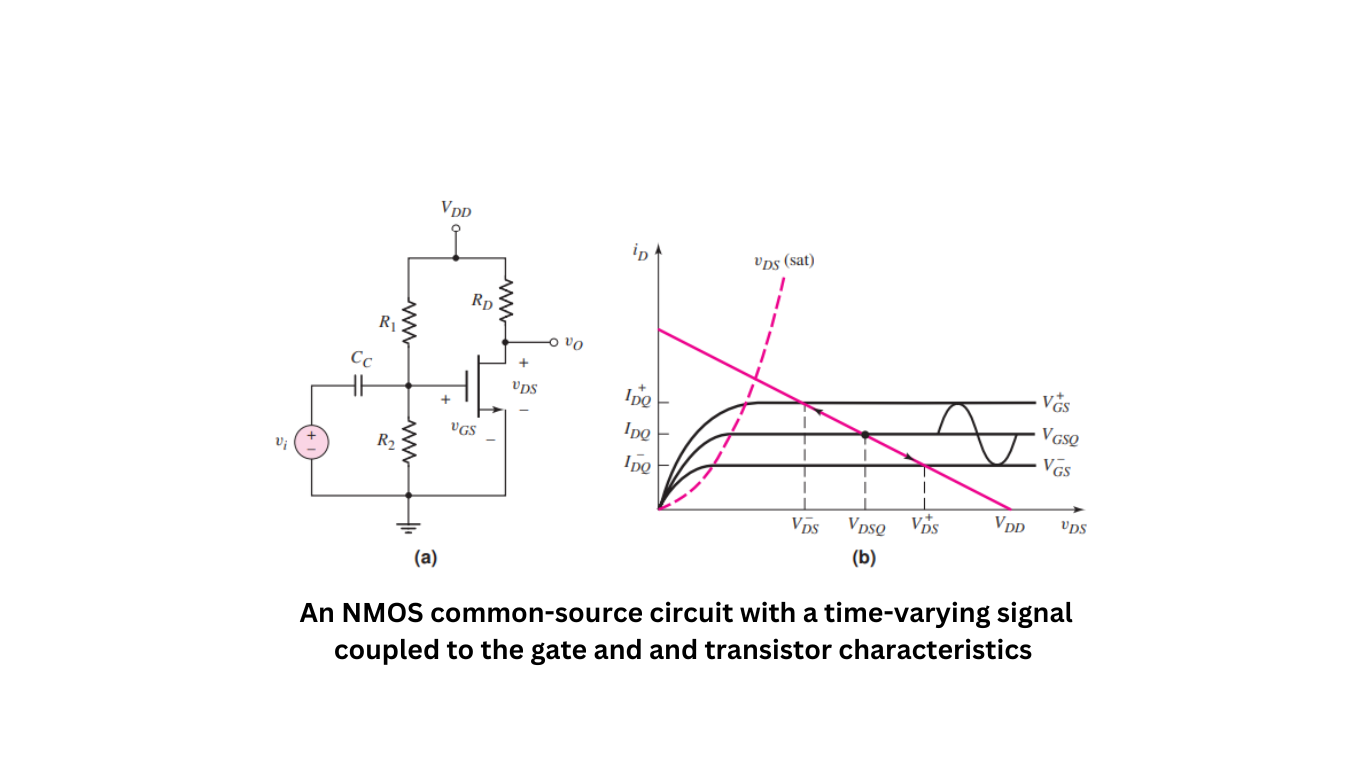
When we combine a MOSFET with other circuit elements, we can use it to amplify small time-varying signals. Figure 1 depicts a MOSFET small-signal amplifier, which is a common-source circuit where a time-varying signal is coupled to the gate using a coupling capacitor. In Figure 1, you can see the transistor characteristics and the load line. The load line is determined when the input voltage (vi) is equal to 0.
Establishing the Q-point
To establish a specific Q-point on the load line, you can design the ratio of the bias resistors R1 and R2 accordingly. If we assume that the input voltage vi = Vi * sin(ωt), the gate-to-source voltage will have a sinusoidal signal superimposed on its DC quiescent value. As the gate-to-source voltage changes over time, the Q-point will move along the load line, as indicated in the figure.
Resulting Signal Amplification
This movement along the load line results in a sinusoidal variation in both the drain current and the drain-to-source voltage. As a consequence, the variation in the output voltage can be larger than the input signal voltage, indicating that the input signal is amplified. The actual signal gain depends on both the transistor parameters and the values of the circuit elements.