
In this article, we will discuss the logic NAND gate, its definition, truth table, Boolean expression, electrical equivalent circuit
What is NAND Gate?

When you use a NAND gate (short for “NOT-AND” gate), you’re working with a logic gate that gives an output signal only when all its input signals are NOT true. Essentially, it’s an AND gate followed by a NOT gate. If you look at the symbol for a NAND gate, you’ll see two input lines entering the gate and a single output line exiting it.
Working on NAND Gate
The operation of a two-input NAND gate for different possible combinations of inputs is as follows:
2-Input NAND Gate
- A = 0 and B = 0, the output Y is 1.
- A = 0 and B = 1, the output Y is 1.
- A = 1 and B = 0, the output Y is 1.
- A = 1 and B = 1, the output Y is 0.
3-Input NAND Gate
The operation of a three-input NAND gate for different possible combinations of inputs is described below:
- A = 0, B = 0, and C = 0, the output Y is 1.
- A = 0, B = 0, and C = 1, the output Y is 1.
- A = 0, B = 1, and C = 0, the output Y is 1.
- A = 0, B = 1, and C = 1, the output Y is 1.
- A = 1, B = 0, and C = 0, the output Y is 1.
- A = 1, B = 0, and C = 1, the output Y is 1.
- A = 1, B = 1, and C = 0, the output Y is 1.
- A = 1, B = 1, and C = 1, the output Y is 0.
The NAND gate is particularly noteworthy because it can be used to construct any other type of logic gate. In this sense, it is considered a universal gate, capable of implementing all logical operations. Additionally, by connecting the output of a NAND gate to one of its inputs, it can function as a logic inverter, providing a logical complement of the input signal.
Applications of NAND Gate: NAND gates find extensive applications in various fields, ranging from digital electronics to computer architecture and beyond. They are essential in building complex logic circuits, such as multiplexers, decoders, and flip-flops. NAND gates are also integral to data storage and memory units, enabling efficient data retrieval and manipulation.
Advantages and Disadvantages of NAND Gate: NAND gates offer several advantages in digital circuit design. They have a simple structure, requiring fewer transistors compared to other gates, which leads to cost savings in integrated circuit fabrication. Furthermore, NAND gates have high noise immunity and exhibit stable behavior even in noisy environments. However, they also have some limitations, such as increased propagation delay and power consumption compared to simpler gates.
NAND Gate in Digital Electronics: In digital electronics, NAND gates play a important role in realizing complex systems. They are extensively used in the design and implementation of arithmetic and mathematical operations, logical functions, and memory units. NAND gates are integrated into digital systems, such as microprocessors, microcontrollers, and application-specific integrated circuits (ASICs), to enable efficient data processing and control.
NAND Gate vs. Other Logic Gates: Comparing NAND gates with other logic gates provides insights into their unique characteristics and functionalities. When compared to AND gates, NAND gates produce the complement of the AND operation, making them particularly useful in specific scenarios. Similarly, NAND gates have distinct advantages over OR gates, providing a versatile logical operation that finds applications in diverse circuit designs.
2-Input NAND Gate Truth Table
| Input | Output | |
| A | B | Y = (AB)’ |
| 0 | 0 | 1 |
| 0 | 1 | 1 |
| 1 | 0 | 1 |
| 1 | 1 | 0 |
3-Input NAND Gate Truth Table
| Input | Output | ||
| A | B | C | Y = (AB)’ |
| 0 | 0 | 0 | 1 |
| 0 | 0 | 1 | 1 |
| 0 | 1 | 0 | 1 |
| 0 | 1 | 1 | 1 |
| 1 | 0 | 0 | 1 |
| 1 | 0 | 1 | 1 |
| 1 | 1 | 0 | 1 |
| 1 | 1 | 1 | 0 |
Realization of Basic Logic Gates using NAND Gate
As we mentioned above that, the NAND gate is a universal logic gate, hence we can implement any basic logic using this NAND gate.
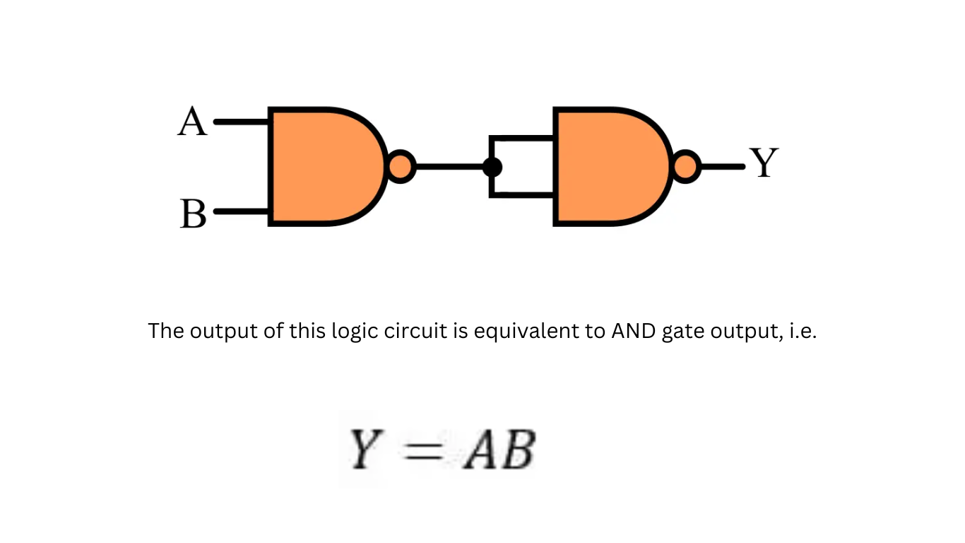
1. AND Gate using NAND Gate
The implementation of an AND gate using a NAND gate is shown in the following figure.
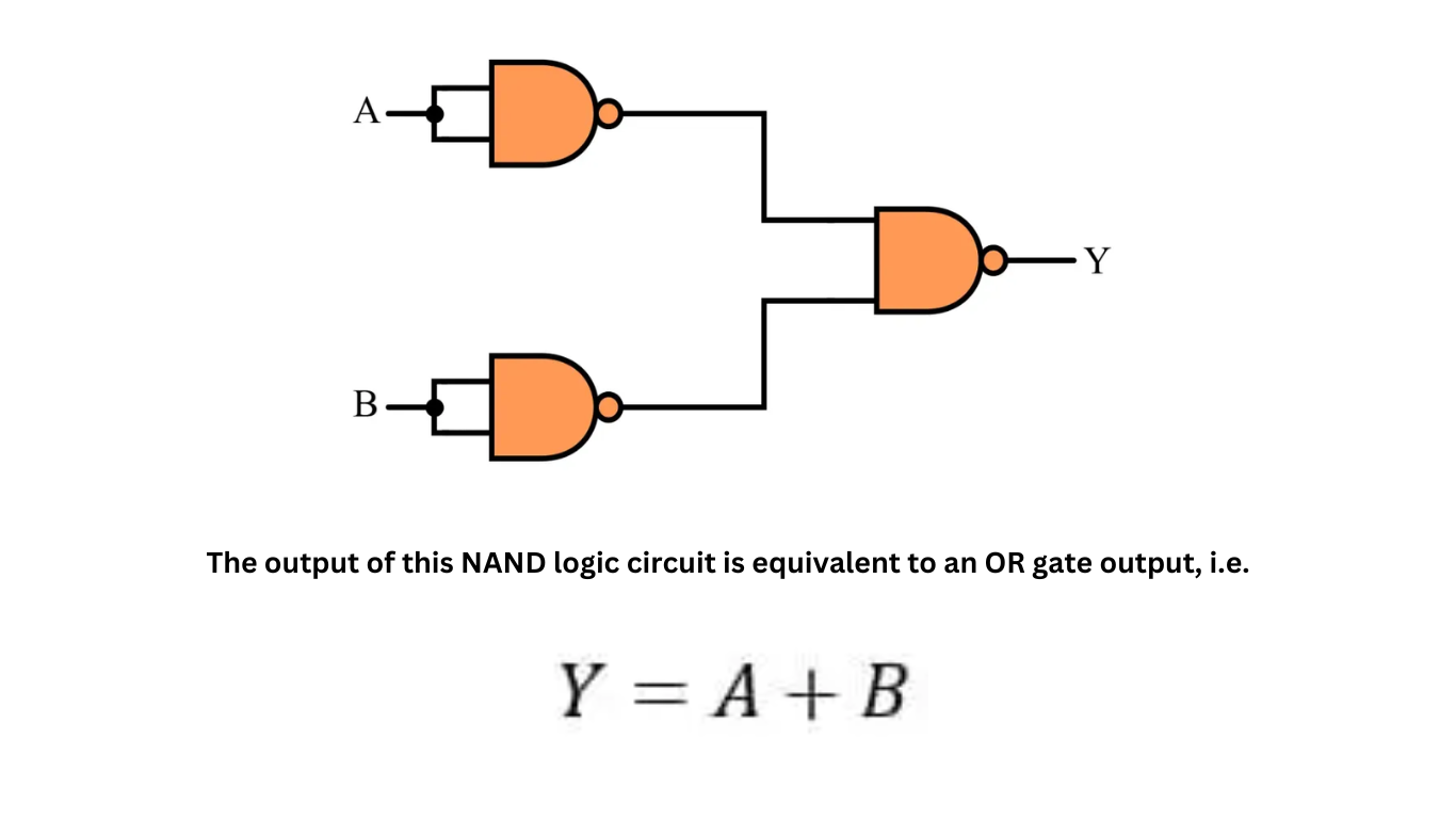
2. OR Gate using NAND Gate
The implementation of an OR Gate using NAND is shown in the following figure.
3. NOT Gate using NAND Gate
The implementation of a NOT gate using a NAND gate is shown in the following figure.

Troubleshooting NAND Gate Circuits: As with any electronic circuitry, NAND gate circuits can encounter issues that require troubleshooting. Understanding common problems, such as incorrect output or improper behavior, is important for effective debugging. By employing testing techniques, such as voltage measurements and logic analyzers, engineers can identify and rectify issues in NAND gate circuits.
Future Developments and Trends: The field of logic gates and digital electronics is continuously evolving. Ongoing research and development efforts aim to enhance NAND gate technology by reducing power consumption, improving speed, and increasing integration density. Emerging applications, such as quantum computing and advanced artificial intelligence systems, present new opportunities for leveraging NAND gates and exploring novel computing paradigms.
In conclusion, the logic NAND gate is a fundamental component in digital electronics, playing a vital role in various applications. Its ability to perform universal logic operations, simplicity in design, and extensive usability make it an essential building block for complex digital systems. As technology advances, the NAND gate is expected to evolve further, enabling innovative solutions and expanding the horizons of digital circuit design.
FAQs
1. Can a NAND gate be used as a substitute for other logic gates?
Yes, a NAND gate can be used as a substitute for any other logic gate, including AND, OR, and NOT gates. It is considered a universal gate capable of implementing all logical operations.
2. Are there any drawbacks to using NAND gates in circuit design?
While NAND gates offer advantages such as simplicity and noise immunity, they also have some limitations. These include increased propagation delay and power consumption compared to simpler gates.
3. What are some practical applications of NAND gates?
NAND gates find applications in various fields, including building complex logic circuits, data storage and memory units, and arithmetic and mathematical operations.
4. How are NAND gates used in troubleshooting circuits?
When troubleshooting NAND gate circuits, engineers employ techniques such as voltage measurements and logic analyzers to identify and rectify issues, such as incorrect output or improper behavior.
5. What does the future hold for NAND gate technology?
Ongoing research aims to improve NAND gate technology by reducing power consumption, increasing speed, and enhancing integration density. Emerging applications, such as quantum computing, present exciting possibilities for leveraging NAND gates in groundbreaking ways.
OR Gate- Symbol, Truth Table, and Circuit Diagram
AND Gate- Symbol, Truth Table, and Circuit Diagram