What is ratioed logic in CMOS circuits?
Ratioed logic is an approach in CMOS circuit design aimed at reducing the number of transistors required to implement a logic function, even though it comes with certain trade-offs. Here’s an overview of ratioed logic, its advantages, and disadvantages compared to complementary CMOS:
Ratioed Logic
Objective: The goal of ratioed logic is to minimize the number of transistors needed to realize a specific logic function.
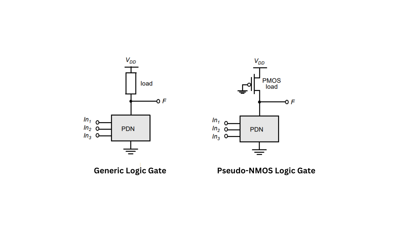
Functionality: Instead of the traditional complementary CMOS approach, which employs both NMOS and PMOS devices for pull-down and pull-up, ratioed logic replaces the entire pull-up network (PUN) with a single load device.
Example: One example of ratioed logic is pseudo-NMOS, which uses a grounded PMOS load device. It significantly reduces the number of transistors compared to complementary CMOS.
Advantages of Ratioed Logic
Fewer Transistors: Ratioed logic typically requires N+1 transistors, whereas complementary CMOS uses 2N transistors, reducing the transistor count.
Nominal High Output Voltage: The high-level output voltage (VOH) is VDD in ratioed logic when the pull-down devices are off (assuming VOL is below VTn).
Disadvantages of Ratioed Logic
Nominal Low Output Voltage: The low-level output voltage (VOL) is not 0 V in ratioed logic because of the competition between the pull-down devices and the grounded PMOS load. This results in reduced noise margins.
Static Power Dissipation: Ratioed logic suffers from static power dissipation when the output is low, as there is a direct current path between VDD and GND. This can lead to increased power consumption in the low-output state.
Trade-offs: Sizing the load device relative to the pull-down devices allows designers to trade off parameters like noise margin, propagation delay, and power dissipation. Achieving the right balance is crucial.
Ratioed vs. Ratioless: Unlike ratioless logic styles, such as complementary CMOS, where the low and high logic levels do not depend on transistor sizes, ratioed logic’s functionality and voltage levels rely on the ratio between NMOS and PMOS sizes. This makes it a “ratioed” logic style.
In summary, ratioed logic offers a reduction in transistor count compared to complementary CMOS, but it comes at the cost of reduced noise margins, static power dissipation, and trade-offs in terms of transistor sizing. Designers need to carefully balance these factors when choosing between ratioed and complementary CMOS logic styles based on the specific requirements of their applications.
What is the primary purpose of the PUN (Pull-Up Network) in complementary CMOS logic?
The primary purpose of the PUN in complementary CMOS logic is to provide a conditional path between VDD and the output when the PDN (Pull-Down Network) is turned off. In contrast, ratioed logic replaces the entire PUN with a single unconditional load device in an attempt to reduce the number of transistors required.
What is the key advantage of pseudo-NMOS logic?
The key advantage of pseudo-NMOS logic is the reduced number of transistors required compared to complementary CMOS logic. This advantage is achieved by using a single NMOS pull-down network for the logic function and a simple PMOS load device. This reduces the transistor count from 2N (complementary CMOS) to N+1.
How does the sizing of the load device in pseudo-NMOS logic impact its performance characteristics?
The sizing of the load device relative to the pull-down devices in pseudo-NMOS logic can be used to trade off parameters such as noise margin, propagation delay, and power dissipation. Smaller load device sizes reduce noise margins but can lead to lower static power dissipation. Larger load device sizes improve noise margins but may increase propagation delay.
Why is the term “ratioed” used to describe pseudo-NMOS logic?
The term “ratioed” is used to describe pseudo-NMOS logic because the voltage swing on the output and the overall functionality of the gate depend on the ratio between the sizes of the NMOS and PMOS transistors. This is in contrast to ratioless logic styles like complementary CMOS, where the low and high levels are independent of transistor sizes.
What is a major disadvantage of pseudo-NMOS logic, particularly when the output is low?
A major disadvantage of pseudo-NMOS logic, especially when the output is low, is the static power dissipation that occurs through a direct current path between VDD and GND. This static power consumption results from the fight between the devices in the PDN and the grounded PMOS load device, leading to increased power consumption in the low-output mode.