
Explain the concept of on-chip Electrostatic Discharge (ESD) protection
Electrostatic discharge (ESD) poses a serious threat to the reliability and functionality of devices within integrated circuit (IC) chips. This phenomenon, caused by the sudden discharge of built-up static charges, can lead to performance degradation or complete failures in ICs. Hence, the implementation of on-chip ESD protection has become a critical consideration in IC design, especially given the escalating demands for higher speeds, smaller devices, and enhanced product reliability.
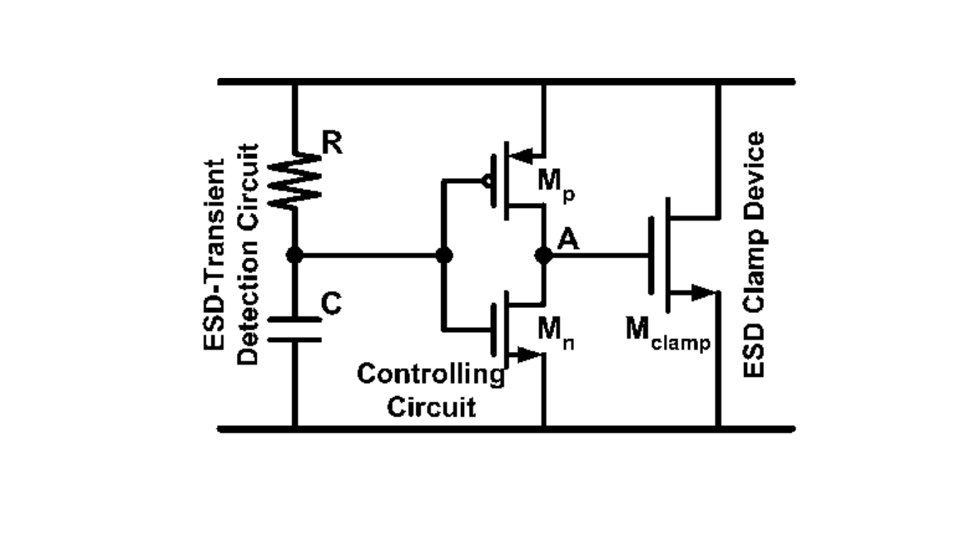
One of the noteworthy approaches to on-chip ESD protection is the utilization of an RC-triggered ESD power clamp circuit. This circuit is engineered to safeguard ICs from ESD events that can potentially cause significant damage. The conventional design of an RC-triggered power clamp circuit encompasses key components such as an N-channel metal oxide semiconductor (NMOS) clamping transistor, an inverter (or a chain of inverters), and an RC (resistor-capacitor) circuit.
NMOS clamping transistor
The NMOS clamping transistor plays a central role in the circuit. It is interconnected between the VDD rail (supply voltage) and the VSS rail (ground). Simultaneously, the RC circuit is linked between these two rails. This RC circuit consists of a resistive element and a capacitor, both placed in series between VDD and VSS. The resistive element can be an NMOS or P-channel metal oxide semiconductor (PMOS) transistor. The output of the inverter is connected to the gate of the NMOS clamping transistor, while the input of the inverter is attached to the output of the RC circuit, positioned at a node between the resistive element and the capacitor.
How does it work?
During normal power-up operations, the rise time of VDD is relatively slow, in the millisecond range. Consequently, the output of the RC circuit aligns with the VDD power rail due to the longer rise time, ensuring that the NMOS clamping transistor remains in an off state. However, during a positive ESD event with a sub-microsecond rise time on the VDD rail, the RC circuit and the inverter collaborate to activate the NMOS clamping transistor. This results in the routing of the ESD current to the VSS rail via the clamping transistor, preventing the ESD from reaching downstream devices. Once the ESD event subsides, the NMOS clamping transistor returns to its off state, facilitating the resumption of normal IC operations.
What is the significance of on-chip ESD protection in IC design?
On-chip ESD protection is critical in IC design due to the increasing demands for higher speeds, smaller devices, and product reliability. ESD events can cause damage to integrated circuit (IC) chips, leading to performance degradation or failures.
What does an RC-triggered ESD power clamp circuit offer in on-chip ESD protection?
An RC-triggered ESD power clamp circuit is a type of ESD protection circuit that helps prevent damage from electrostatic discharge. It includes components like an N-channel metal oxide semiconductor (NMOS) clamping transistor, an inverter, and an RC circuit.
How does the NMOS clamping transistor function in an RC-triggered power clamp circuit?
The NMOS clamping transistor is connected between the VDD rail (power supply voltage) and the VSS rail (ground). It turns on during an ESD event to route the ESD current to the VSS rail, protecting downstream devices.
What role does the RC circuit play in an RC-triggered power clamp circuit?
The RC circuit includes a resistive element (NMOS or PMOS transistor) and a capacitor connected in series between the VDD rail and VSS rail. It contributes to the circuit’s response time during an ESD event.
Under what conditions does the NMOS clamping transistor remain off in an RC-triggered power clamp circuit?
During normal operation, when the rise time of VDD is longer than the RC delay of the circuit, the output of the RC circuit is at the same potential as the VDD power rail. As a result, the NMOS clamping transistor remains off.
How does the RC-triggered power clamp circuit respond to a positive ESD event on the VDD rail?
When a positive ESD event with a sub-microsecond rise time occurs on the VDD rail, the RC circuit and inverter activate. This turns on the NMOS clamping transistor, directing the ESD current to the VSS rail to protect downstream devices.
What concerns are associated with the conventional RC-triggered power clamp circuit?
The conventional circuit may experience false triggering of the NMOS clamping transistor during normal operations due to voltage overshoot or fast VDD power-up rise times. Additionally, the relatively short RC time constant limits the discharge time for ESD.
Why is a longer RC time constant desired in an ESD protection circuit?
A longer RC time constant allows for more time to discharge ESD through the NMOS clamping transistor, enhancing protection. However, achieving a longer time constant by increasing the capacitor size can be impractical due to chip space constraints.
What challenges does the conventional RC-triggered circuit face in terms of capacitor size?
Increasing the capacitor size to achieve a longer RC time constant requires valuable chip real estate, making this solution impractical for ESD protection.
What is the need addressed by an improved RC-triggered power clamp circuit?
An improved RC-triggered power clamp circuit addresses the need for effective ESD protection with, reduced false triggering and an increased RC time constant, without the requirement for excessive chip area.