
Resistive Load Inverter
An inverter is used to convert logic levels, specifically from logic ‘0’ to logic ‘1’ and vice versa.
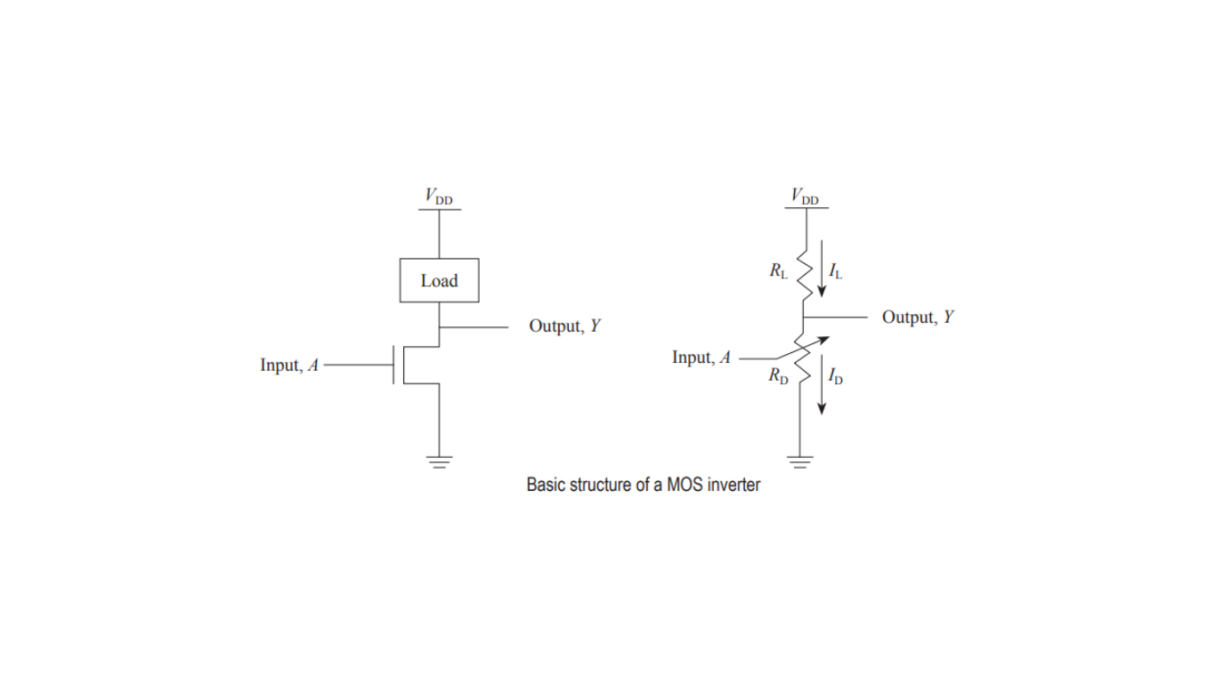
Basic Structure of a MOS Inverter
The MOS inverter consists of two key components:
An nMOS (n-type Metal-Oxide-Semiconductor) transistor: This transistor is connected between the output node and the ground. It’s controlled by the voltage applied to its gate terminal.
A load: The load is connected between the power supply voltage (VDD) and the output terminal.
Inverter Operation
When the input voltage is low (representing logic ‘0’), the nMOS transistor is turned OFF. In this state, the output is connected to the power supply (VDD) through the load. The load can be either a resistor or another MOS transistor.
Conversely, when the input is high (representing logic ‘1’), the nMOS transistor becomes ON. This connects the output to the ground terminal.
Output Voltage Levels
The output voltage levels for logic ‘0’ and logic ‘1’ are determined by the characteristics of the load and the driver nMOS transistor. These levels can be calculated using the following expression:
Vout = VDD * (RD / (RD + RL))
For logic ‘0’ input, which should yield a logic ‘1’ output, either RL (the load resistance) should be zero, or RD (the resistance of the driver nMOS transistor) should be infinite. In this way, Vout approaches VDD.
For logic ‘1’ input, which should result in a logic ‘0’ output, either RL should be infinite, or RD should be zero, causing Vout to approach 0.
The disadvantage of a resistive inverter is that it requires a large area of silicon in order to implement the resistive load.
In summary, the MOS inverter is a critical component in digital circuits, responsible for logical inversion. Its output voltage levels are determined by the input and the characteristics of the load and driver transistor. For logic ‘0’ input, Vout should be close to VDD, while for logic ‘1’ input, Vout should be close to 0. These properties make it a fundamental element in digital logic design.