
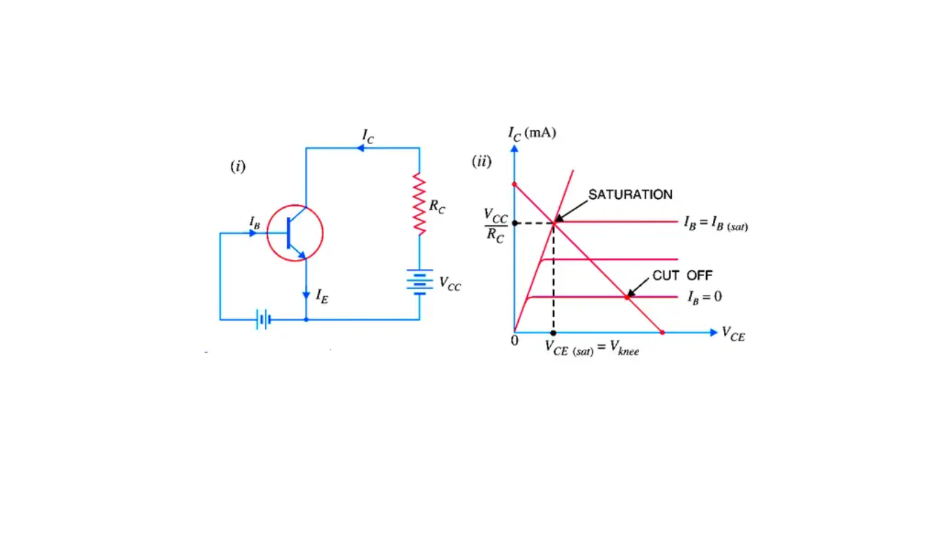
Saturation and Cutoff Region in CMOS
The saturation and cutoff regions in CMOS are important for understanding how MOSFETs behave under different voltage conditions. NMOS and PMOS transistors can operate in cutoff, linear (triode), and saturation regions depending on their terminal voltages.
These operating regions determine whether a transistor behaves approximately as an open switch, voltage-controlled current source, or low-resistance path.
Understanding these regions is essential for CMOS inverter analysis, analog circuits, digital logic, transistor sizing, and VLSI design.

What Are MOSFET Operating Regions?
A MOSFET can operate in different regions depending mainly on its gate-to-source voltage (VGS) and drain-to-source voltage (VDS).
For an NMOS transistor, the commonly discussed regions are:
- Cutoff region
- Linear or triode region
- Saturation region
The PMOS transistor has corresponding regions, but the voltage conditions are expressed using the appropriate PMOS polarities or source-referenced voltages.
These regions are useful because they tell us how the transistor responds to applied voltages.
CMOS Technology
CMOS (Complementary Metal-Oxide-Semiconductor) technology uses complementary NMOS and PMOS transistors to implement digital logic.
A typical CMOS inverter contains:
- One PMOS transistor
- One NMOS transistor
- A common input connected to both gates
- A common output connected to both drains
- PMOS source connected toward VDD
- NMOS source connected toward ground
The complementary operation of these transistors allows CMOS logic to achieve:
- Low static power consumption
- High noise immunity
- Full logic swing
- High integration density
- Good scalability
Cutoff Region of a MOSFET
The cutoff region is the operating condition in which the MOSFET’s channel is not formed strongly enough to support significant normal channel current.
For an NMOS, the simplified condition is:
VGS < VTH
where:
- VGS = gate-to-source voltage
- VTH = threshold voltage
Under this condition, the transistor is considered OFF in the ideal long-channel model.
Therefore:
NMOS cutoff → transistor OFF → very small channel current
The actual device can still have leakage currents, so “zero current” is an idealization.
NMOS Cutoff
For an NMOS:
VGS < VTH
The inversion channel is not established sufficiently for normal conduction.
The transistor therefore behaves approximately like an open switch.
For example, in a CMOS inverter when:
Vin = 0
the NMOS is normally in cutoff.
PMOS Cutoff
For a PMOS, the corresponding condition is based on the magnitude of its gate-to-source voltage.
A simplified representation is:
VSG < |VTHP|
where VSG is the source-to-gate voltage.
Under this condition, the PMOS is OFF.
For a CMOS inverter when:
Vin = VDD
the PMOS is normally in cutoff.
Saturation Region of a MOSFET
The saturation region is different from the low-resistance ON-state commonly associated with a digital switch.
For an NMOS in the long-channel model, saturation occurs approximately when:
VGS > VTH
and
VDS ≥ VGS − VTH
In this region, increasing VDS further has a relatively limited effect on the ideal long-channel drain current compared with the linear region.
The transistor can therefore behave approximately as a voltage-controlled current source.
This makes the saturation region particularly important in:
- Analog amplifiers
- Current mirrors
- Differential pairs
- Bias circuits
- Analog CMOS design
Important correction: A MOSFET in saturation should not be described simply as a “fully ON, low-resistance channel.” The low-resistance behavior is associated more closely with the linear/triode region. Saturation is the region commonly used for current-source and amplifier operation.
NMOS Saturation Condition
For an NMOS:
VGS > VTH
and
VDS ≥ VGS − VTH
The ideal long-channel saturation current can be approximated by:
ID = ½ μnCox(W/L)(VGS − VTH)²
where:
- ID = drain current
- μn = electron mobility
- Cox = oxide capacitance per unit area
- W = transistor width
- L = transistor length
- VTH = threshold voltage
This simplified equation assumes an ideal long-channel MOSFET and ignores effects such as channel-length modulation.
Linear or Triode Region
The linear region is important because it completes the picture of MOSFET operation.
For an NMOS:
VGS > VTH
and
VDS < VGS − VTH
In this region, the transistor behaves approximately like a voltage-controlled resistor for sufficiently small VDS.
The drain current in the long-channel model is approximately:
ID = μnCox(W/L)[(VGS − VTH)VDS − VDS²/2]
This region is heavily used when a MOSFET operates as a switch in digital circuits.
Saturation vs Linear vs Cutoff
| Region | NMOS Condition | Approximate Behavior |
|---|---|---|
| Cutoff | VGS < VTH | OFF / very small channel current |
| Linear/Triode | VGS > VTH and VDS < VGS − VTH | Voltage-controlled resistive path |
| Saturation | VGS > VTH and VDS ≥ VGS − VTH | Voltage-controlled current source |
This distinction is very important in CMOS circuit analysis.
How Do These Regions Apply to a CMOS Inverter?
A CMOS inverter is a particularly useful example because the NMOS and PMOS can occupy different operating regions depending on the input voltage.
Consider a CMOS inverter with:
Vin = 0
The NMOS is OFF, while the PMOS is ON.
The output is therefore pulled toward:
VDD
When:
Vin = VDD
the PMOS is OFF, while the NMOS is ON.
The output is therefore pulled toward:
GND
During the transition between these two input conditions, both transistors can conduct.
CMOS Inverter at Low Input
When:
Vin = 0
For the NMOS:
VGS = 0
Therefore, the NMOS is in cutoff.
For the PMOS, the gate is low relative to its source, so it is ON.
The PMOS pulls the output toward VDD.
Therefore:
Vin = 0 → Vout ≈ VDD
This represents logic 1 at the output.
CMOS Inverter at High Input
When:
Vin = VDD
The NMOS is ON and pulls the output toward ground.
The PMOS is OFF.
Therefore:
Vin = VDD → Vout ≈ 0
This represents logic 0 at the output.
Again, the exact operating region of the ON transistor depends on the instantaneous output voltage.
What Happens During the Transition?
This is where the behavior becomes more interesting.
When Vin moves from low to high:
- The PMOS begins turning OFF.
- The NMOS begins turning ON.
- Both devices can conduct simultaneously.
- The output voltage starts falling.
- The transistor operating regions change as the output voltage changes.
Similarly, when Vin moves from high to low, the complementary behavior occurs.
Therefore, it is not technically correct to say that a CMOS inverter simply has both transistors in saturation during the switching operation.
The operating region of each MOSFET changes continuously with the input and output voltages.
Saturation Region vs Cutoff Region
The two regions represent very different transistor behaviors.
| Characteristic | Cutoff | Saturation |
|---|---|---|
| Channel conduction | Very small | Significant |
| Transistor state | OFF | ON |
| Ideal channel current | Approximately zero | Controlled by VGS |
| Typical use | Switching OFF | Amplification/current source |
| Digital interpretation | Open switch | Depends on circuit |
| Analog importance | Low | Very high |
The terms ON and OFF are useful for digital circuits, but they should not be directly equated with saturation and cutoff in every situation.
Why Is Saturation Important in CMOS?
Saturation is particularly important in analog CMOS circuits.
When a MOSFET operates in saturation, its drain current is primarily controlled by its gate-to-source voltage in the ideal long-channel model.
This allows the transistor to be used for:
- Amplification
- Current mirrors
- Differential amplifiers
- Bias circuits
- Active loads
- Operational amplifiers
The transistor’s transconductance is also an important parameter in this region.
Why Is Cutoff Important in CMOS?
Cutoff is fundamental to digital CMOS operation.
When a transistor is OFF, it ideally blocks the normal channel-current path.
This enables CMOS gates to implement switching functions while maintaining very low static power in the idealized steady-state model.
For example, in a CMOS inverter:
Input low → NMOS OFF
Input high → PMOS OFF
This complementary operation prevents a continuous direct path from VDD to ground in the ideal steady state.
In real CMOS circuits, however, leakage currents are always present to some degree.
Transistor Sizing and Operating Regions
Transistor dimensions strongly influence CMOS circuit behavior.
Two important dimensions are:
- Width (W)
- Length (L)
The ratio:
W/L
has a major effect on transistor drive strength.
Increasing transistor width generally increases the available drive current, while changing transistor length affects current, capacitance, short-channel behavior, and other device characteristics.
Proper sizing can help optimize:
- Propagation delay
- Rise and fall times
- Power consumption
- Noise margins
- Drive strength
- Switching behavior
Therefore, transistor sizing must be considered together with the desired operating conditions.
Saturation and Cutoff in Analog vs Digital CMOS
The meaning and importance of these regions depend on the application.
In Analog CMOS
Designers often intentionally bias MOSFETs in saturation to obtain:
- High output resistance
- Useful transconductance
- Voltage gain
- Current-source behavior
In Digital CMOS
Designers are usually more concerned with whether transistors provide effective:
- Pull-up paths
- Pull-down paths
- Low resistance
- Fast switching
During switching, a transistor can pass through multiple operating regions.
Therefore, digital CMOS design should not be described simply as cutoff versus saturation.
Common Misconceptions
1. Saturation Means the MOSFET Is Fully ON
Not necessarily.
For a MOSFET, saturation is a specific operating region defined by voltage conditions.
A MOSFET used as a low-resistance switch is generally operated in the linear/triode region when it is strongly ON.
2. Cutoff Means Absolutely Zero Current
In the ideal MOSFET model, cutoff means the channel current is approximately zero.
Real devices still have leakage mechanisms such as:
- Subthreshold leakage
- Junction leakage
- Gate leakage
- GIDL
Therefore, practical OFF-state current is not exactly zero.
3. CMOS Inverter Always Has One Transistor in Saturation
This is an oversimplification.
During the inverter transition, both devices can conduct and their operating regions change with Vin and Vout.
4. Saturation and Active Region Always Mean Different Things
Terminology can vary between device types and textbooks.
For MOSFETs, saturation region is the standard term for the region used for current-source/amplifier operation.
The term active region is more commonly associated with BJTs, although some MOSFET literature may use different terminology.
For clarity, it is better to use cutoff, linear/triode, and saturation when discussing MOSFET operating regions.
Frequently Asked Questions
What is the cutoff region in a MOSFET?
Cutoff is the operating region where the gate voltage is insufficient to establish normal channel conduction. For an NMOS, the simplified condition is VGS < VTH.
What is the saturation region in a MOSFET?
Saturation is the region where the MOSFET operates as a voltage-controlled current source in the ideal long-channel model. For an NMOS, the simplified condition is VGS > VTH and VDS ≥ VGS − VTH.
Is saturation the same as the fully ON state?
No. A MOSFET operating as a low-resistance switch is generally associated with the linear/triode region, not saturation.
Which region is used for MOSFET amplification?
The saturation region is commonly used for MOSFET amplification because it provides useful transconductance and output resistance.
Which region represents an OFF transistor?
The cutoff region represents the OFF state in the idealized MOSFET model.
Do CMOS transistors consume zero power in cutoff?
No. The ideal channel current is approximately zero, but real CMOS transistors have leakage currents.
Can both NMOS and PMOS conduct at the same time?
Yes. During the transition of a CMOS inverter, both devices can conduct simultaneously.
Key Takeaways
- MOSFETs commonly operate in cutoff, linear/triode, and saturation regions.
- Cutoff corresponds to the transistor being OFF in the idealized model.
- Linear/triode operation provides low-resistance behavior useful for switching.
- Saturation is commonly used for amplification and current-source behavior.
- Saturation should not be described simply as a fully ON, low-resistance state.
- A CMOS inverter can have both NMOS and PMOS conducting during the transition.
- The operating region of each transistor depends on its terminal voltages.
- Transistor sizing affects current, speed, power, and switching behavior.
- Real MOSFETs have leakage even when they are nominally in cutoff.
- Understanding these regions is essential for CMOS, analog design, digital design, and VLSI analysis.