
Scan-Based Techniques
The scan-based design focuses on connecting these storage elements to form a long serial shift register, commonly known as a scan path.In a general sense, a sequential circuit consists of a combinational circuit accompanied by storage elements. This is achieved by utilizing multiplexors and a mode control signal, as illustrated in Figure 1.
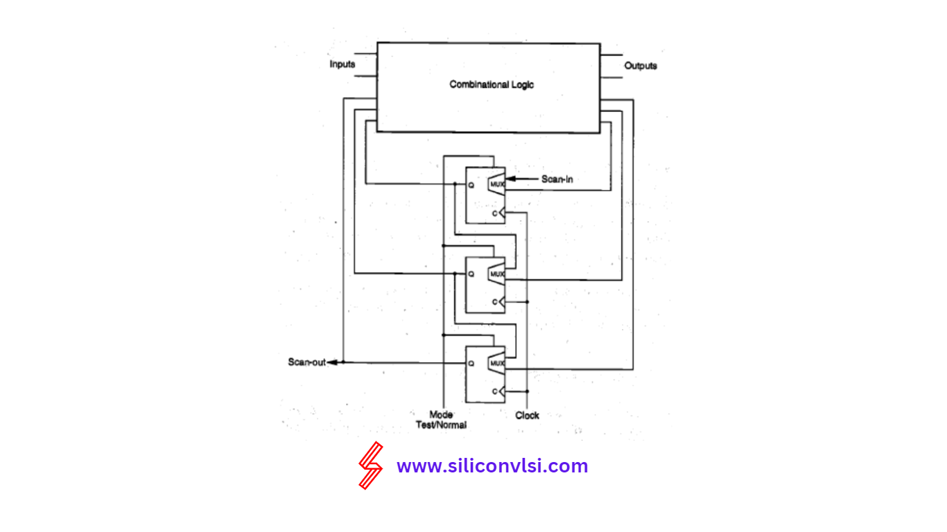
The Role of the Test Mode
During the test mode, the scan-in signal is clocked into the scan path, while the output of the last-stage latch is scanned out. This configuration allows for comprehensive testing of the sequential circuit. Conversely, in the normal mode, the scan-in path is disabled, and the circuit operates as a standard sequential circuit. The testing sequence for scan-based design can be outlined as follows:
- Setting the mode to test and allowing latches to accept data from the scan-in input.
- Verifying the scan path by shifting the test data in and out.
- Scanning in (shifting in) the desired state vector into the shift register.
- Applying the test pattern to the primary input pins.
- Setting the mode to normal and observing the primary outputs of the circuit after sufficient propagation time.
- Asserting the circuit clock for one machine cycle to capture the outputs of the combinational logic into the registers.
- Returning to the test mode, scanning out the register contents, and simultaneously scanning in the next pattern.
- Repeating steps 3-7 until all test patterns have been applied.
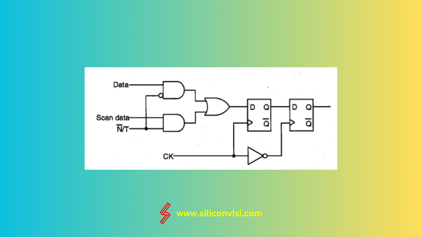
What is Optimizing Storage Cells in Scan Design
To ensure race-free operation, various types of storage cells can be implemented in scan design, such as edge-triggered D flip-flops, master-slave flip-flops, or level-sensitive latches controlled by complementary clock signals. Figure 2 showcases an example of a scan-based design utilizing an edge-triggered D flip-flop. In large high-speed circuits, optimizing a single clock signal for both normal and shift operations can be challenging. To overcome this hurdle, separate clocks are utilized for each operation. Since the shift operation does not require the same speed as the normal operation, its clock can be less constrained.
Level-Sensitive Scan Design: Among the various scan-based design techniques, level-sensitive scan design (LSSD) stands out as an important approach. LSSD combines level sensitivity and the scan path approach through the utilization of shift registers. Level sensitivity ensures that the response of the sequential circuit remains independent of transient characteristics, including component and wire delays. By eliminating hazards