
What is a Set-Reset (SR) Flip-flop?
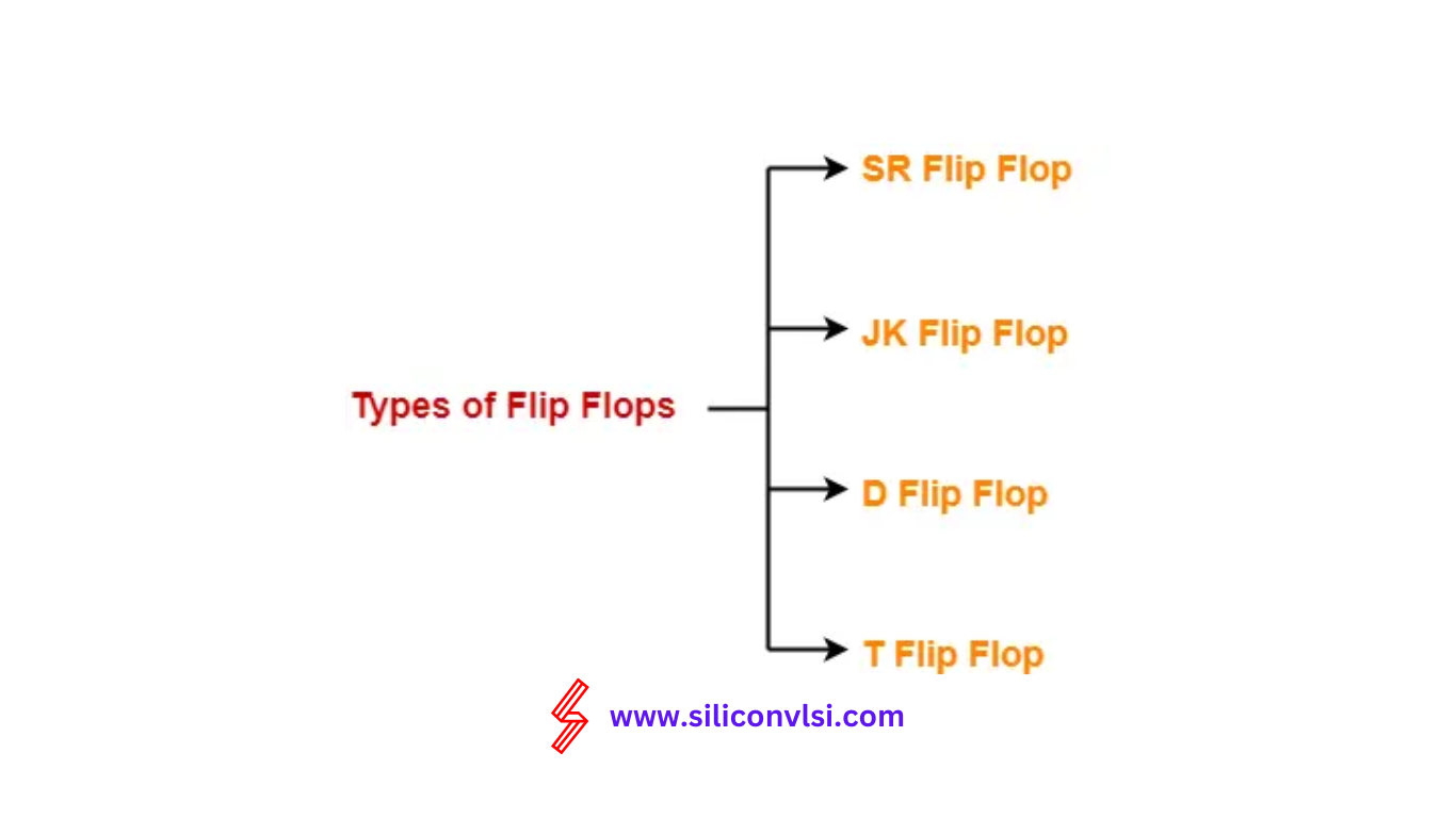
Before we dive into the topic, it’s important to have a basic understanding of flip-flops. If you’re unfamiliar, flip-flops are memory elements that store a single bit of information, which makes them essential in digital circuits. In this discussion, we’ll focus on the SR flip-flop — also called the Set-Reset flip-flop — which is the simplest of the four basic types. Together, we’ll explore its construction, logic circuits, truth table, characteristic equation, and excitation table.
Construction of SR Flip Flop
There are two methods for constructing an SR flip flop: using a NOR latch or using a NAND latch. Both methods involve utilizing specific logic gates to achieve the desired functionality.
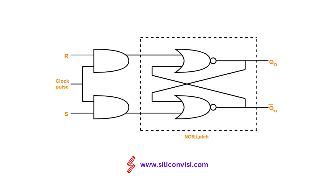
SR Flip Flop By Using NOR Latch
The first method employs a NOR latch and two AND gates to create the SR flip-flop. The logic circuit for this construction is as follows:
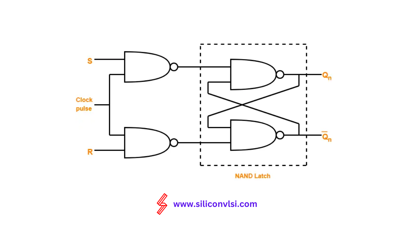
SR Flip Flop By Using NAND Latch
The second method utilizes a NAND latch and two NAND gates for constructing the SR flip flop. The logic circuit for this construction is as shown below:
Logic Symbol
The logic symbol for the SR flip-flop is represented as follows:
[Insert Logic Symbol Image for SR Flip Flop]Truth Table
The truth table provides a comprehensive representation of the behavior and outputs of the SR flip-flop based on its inputs. The truth table for the SR flip-flop is as follows:
To simplify the truth table, we can reduce it to a more concise form. The reduced truth table for the SR flip-flop is as follows:
| Qn | Qn+1 | S | R |
| 0 | 0 | 0 | X |
| 0 | 1 | 1 | 0 |
| 1 | 0 | 0 | 1 |
| 1 | 1 | X | 0 |
Excitation Table
Equation 0f SR flip-flop
The characteristic equation of the SR flip-flop can be derived from the truth table. By analyzing the inputs and outputs, we can formulate the following characteristic equation:
Qn+1 = S + QnR’
The excitation table provides valuable insights into the required inputs for a given combination of the present state (Qn) and the next state (Qn+1). It helps determine the necessary values of S and R for specific state transitions. The excitation table for the SR flip-flop is as follows:
Conclusion
Understanding the construction and functionality of the SR flip-flop is essential for anyone working with digital circuits. By grasping the concepts discussed in this article, you can effectively utilize the SR flip-flop in your designs and develop efficient and reliable systems.