

D Flip-Flop Using MUX: 7 Powerful Steps to Design It
A D flip-flop using MUX is a useful way to understand how a fundamental sequential circuit can be constructed from multiplexers.
A D flip-flop, commonly called a DFF, stores one bit of binary information and updates its output according to the input data and clock signal. It is one of the most widely used sequential elements in digital and VLSI design.
The D flip-flop is especially important because it provides a simple data path: the designer mainly controls a single D input to determine the next state of the flip-flop.
In this article, we will understand the D flip-flop truth table, its operation, how a D flip-flop can be implemented using 2:1 multiplexers, and its applications in VLSI design.
D Flip-Flop Truth Table
A D flip-flop is normally an edge-triggered device. For a positive-edge-triggered D flip-flop, the output changes on the rising edge of the clock.
The basic characteristic is:
Q(next) = D
at the active clock edge.
The truth table can therefore be represented as:
| Clock Condition | D | Q(next) |
|---|---|---|
| No active clock edge | 0 | Q |
| No active clock edge | 1 | Q |
| Rising edge | 0 | 0 |
| Rising edge | 1 | 1 |
Here, Q represents the previous output state and Q(next) represents the updated state after the active clock edge.
This is an important distinction from a level-sensitive latch. A flip-flop responds to its specified clock edge rather than continuously following the data input while the clock is at a particular logic level.
What Is a D Flip-Flop?
A D flip-flop is a sequential logic element that stores one bit of information.
It generally has:
- D — Data input
- CLK — Clock input
- Q — Output
- Q̅ — Complementary output
For a positive-edge-triggered device, the D input is sampled at the rising edge of the clock.
If:
D = 0
at the active clock edge, then:
Q(next) = 0
If:
D = 1
at the active clock edge, then:
Q(next) = 1
After the clock edge, the output remains stored until the next active edge.
How Does a D Flip-Flop Work?
The basic operation is very simple.
Suppose the current output is:
Q = 0
If the data input is changed to:
D = 1
the output does not immediately have to change.
When the next active clock edge occurs, the flip-flop samples the input.
The new state becomes:
Q(next) = 1
Similarly, if:
D = 0
at the next active edge, the output becomes:
Q(next) = 0
Therefore, the D input determines the next state, while the clock determines when that state is captured.
This property makes the D flip-flop particularly convenient for sequential circuit design.
Why Is the D Flip-Flop Widely Used in VLSI?
D flip-flops are extensively used in synchronous digital systems.
One important advantage is the simple relationship between the data input and the next state.
For a typical sequential circuit:
D = Next State Logic
The designer calculates the required next state and connects that logic to the D input.
This simplifies the design of:
- Registers
- Counters
- Pipeline stages
- Finite state machines
- Shift registers
- Synchronizers
- Sequential datapaths
The simple data interface also makes DFF-based standard-cell libraries convenient for automated VLSI implementation.
What Is a Multiplexer?
Before understanding the DFF implementation, it is useful to understand the basic operation of a multiplexer.
A multiplexer, or MUX, is a combinational circuit that selects one of several input signals and transfers the selected signal to its output.
A 2:1 MUX has:
- Two data inputs
- One select input
- One output
Its inputs can be represented as:
- I0
- I1
- S
- Y
The output equation is:
Y = S̅I0 + SI1
When:
S = 0
the output is:
Y = I0
When:
S = 1
the output is:
Y = I1
Because a MUX can select between different signals, it can be used to implement many types of combinational and sequential logic structures.
D Flip-Flop Using MUX
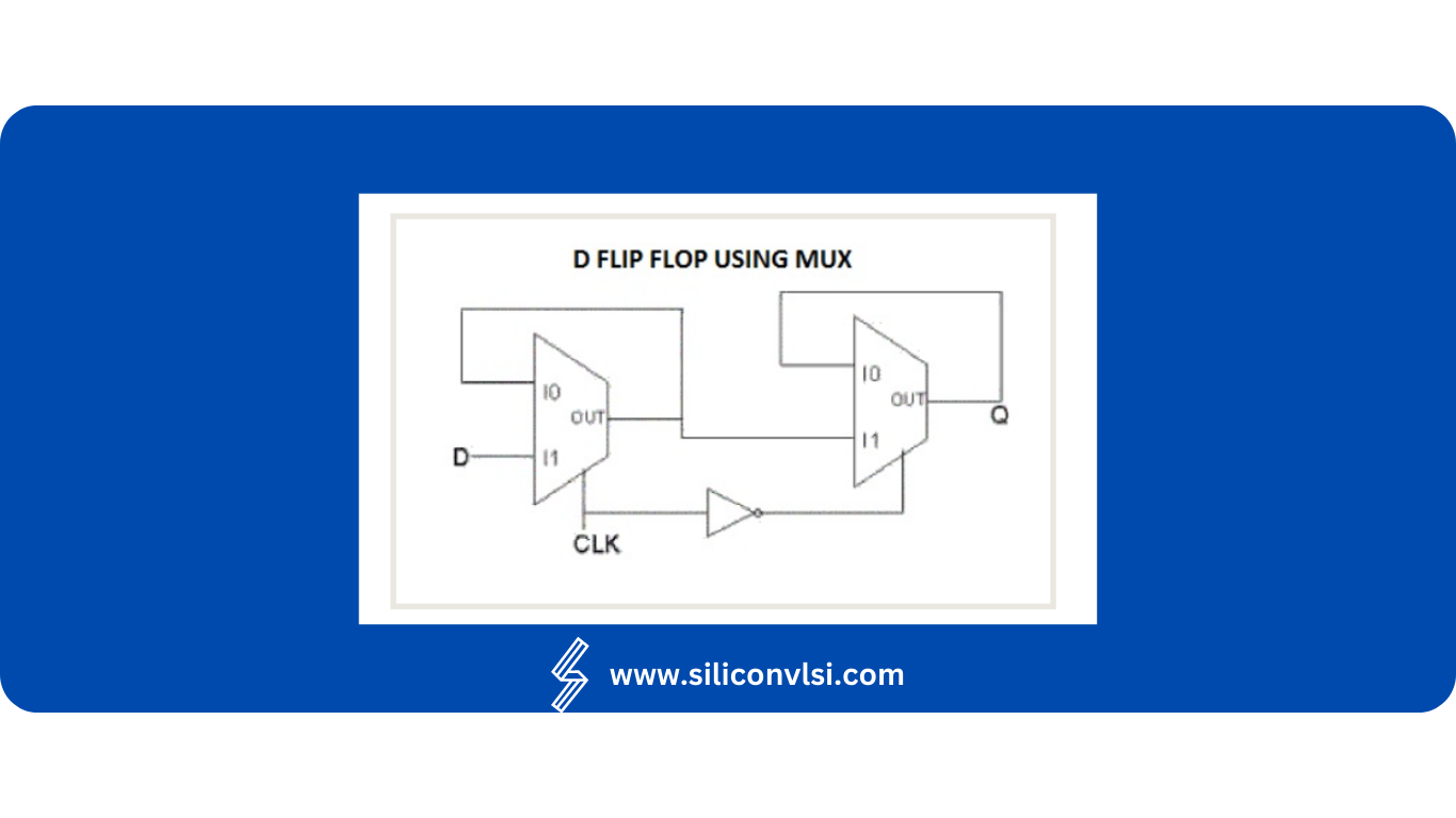
A D flip-flop can be constructed conceptually using multiplexers arranged to provide storage and feedback.
The key idea is that a MUX can select between:
- A new data value
- A previously stored value
When the circuit is arranged appropriately with feedback and clock-controlled selection, the previous state can be retained or a new state can be transferred.
A practical implementation may use two 2:1 multiplexers arranged as a master-slave structure.
D Flip-Flop Using Two 2:1 MUXes
A common conceptual implementation uses two 2:1 multiplexers.
The first MUX forms the master storage stage, while the second MUX forms the slave storage stage.
The two stages operate with complementary clock phases so that the circuit behaves as an edge-triggered storage element.
The basic idea is:
Master stage → Slave stage → Q
The master captures the input during one clock phase, while the slave transfers the stored value during the opposite phase.
This arrangement prevents the output from continuously following the D input.
How to Design a D Flip-Flop Using MUX
The implementation can be understood through the following steps.
Step 1: Start With the D Input
The D input represents the data that must be stored.
The objective of the circuit is to transfer this data to Q at the appropriate clock edge.
Therefore, D becomes the data source for the storage structure.
Step 2: Use a 2:1 MUX for Data Selection
A 2:1 MUX can select between the incoming data and a feedback signal.
The feedback path represents the previously stored state.
This is important because a sequential circuit must have the ability to retain its previous value.
Conceptually:
New data → MUX
Previous state → MUX
The select signal determines which value is passed forward.
Step 3: Create the Storage Structure
A single combinational MUX by itself cannot store information.
Storage is obtained by incorporating feedback and controlled storage stages.
In a master-slave implementation, two storage stages are connected sequentially.
The first stage captures the data during one clock phase.
The second stage transfers the captured value to the output during the opposite phase.
Step 4: Apply the Clock Signal
The clock controls when each stage is transparent and when it holds its state.
For a positive-edge-triggered implementation, the master and slave stages operate on complementary clock phases.
This allows the final output to change at the desired clock edge.
Step 5: Connect the Feedback
Feedback is necessary for retaining the stored state.
When the circuit is not accepting new data, the existing state is maintained.
This can be viewed conceptually as:
Q → Feedback → Storage stage
The feedback path allows the circuit to preserve its previous value.
Step 6: Obtain the Q Output
The output of the final storage stage becomes:
Q
At the active clock edge, the value captured from D appears at the output.
Therefore:
Q(next) = D
Step 7: Verify the Operation
Finally, verify the circuit for both possible data values.
If:
D = 0
then after the active clock edge:
Q = 0
If:
D = 1
then after the active clock edge:
Q = 1
This confirms the basic D flip-flop behavior.
Master-Slave Operation
The master-slave structure is an important concept when implementing an edge-triggered DFF.
The two storage stages are controlled by complementary clock phases.
For example, in a positive-edge-triggered arrangement:
- During the low clock phase, the master stage can capture the input.
- At the rising edge, the master closes and the slave becomes active.
- The slave transfers the captured value to the output.
- During the high clock phase, the output remains stable.
The exact MUX arrangement and clock polarity depend on the circuit implementation.
The important concept is that the two stages prevent the input from propagating directly to the output throughout the clock cycle.
Why Are Two MUXes Useful?
Using two MUX-based storage stages provides a way to create edge-triggered behavior.
A single MUX is only a combinational element.
It cannot independently provide the complete storage behavior required from a flip-flop.
By combining MUX selection, feedback, and complementary clock phases, a sequential storage structure can be created.
This illustrates an important digital-design principle:
Combinational logic + feedback + clock control → Sequential behavior
D Flip-Flop Using MUX: Working Example
Consider the following sequence.
Initially:
Q = 0
Now assume:
D = 1
The input value is presented to the storage structure.
At the appropriate clock edge, the value of D is captured.
Therefore:
Q(next) = 1
Now change:
D = 0
The output does not immediately change merely because D changed.
At the next active clock edge, the new value is captured.
Therefore:
Q(next) = 0
This demonstrates the storage behavior of the flip-flop.
Characteristic Equation of a D Flip-Flop
The characteristic equation of a D flip-flop is:
Q(next) = D
This is one of the simplest characteristic equations among commonly used flip-flops.
For comparison:
D flip-flop:
Q(next) = D
The simplicity of this relationship is one reason D flip-flops are widely used in synchronous digital systems.
D Flip-Flop vs D Latch
A D flip-flop should not be confused with a D latch.
| Feature | D Latch | D Flip-Flop |
|---|---|---|
| Control | Enable/clock level | Clock edge |
| Operation | Level sensitive | Edge triggered |
| Data behavior | Can follow input during active level | Samples input at active edge |
| Common use | Storage and timing structures | Synchronous sequential circuits |
A latch may remain transparent while its enable signal is active.
A flip-flop instead samples the input at a specified clock edge.
Advantages of Using D Flip-Flops
D flip-flops offer several advantages in digital and VLSI design.
Simple Data Interface
Only one main data input needs to be controlled to determine the next state.
Easy State Design
The relationship:
Q(next) = D
makes next-state implementation straightforward.
Suitable for Synchronous Design
DFFs work naturally with clocked digital systems.
Useful for Pipeline Design
A chain of DFFs can separate combinational logic into pipeline stages.
Useful for Registers
Multiple DFFs can store multiple bits of information.
Convenient for RTL Design
DFFs map naturally to sequential logic described in hardware description languages.
Applications of D Flip-Flops
D flip-flops are used in many digital systems.
1. Data Storage
A DFF can store one bit of binary information.
Multiple DFFs can therefore be combined to create multi-bit storage structures.
2. Registers
A group of DFFs can form a register.
For example, eight DFFs can store an 8-bit value.
Larger registers can be constructed in the same way.
3. Pipeline Registers
DFFs are commonly placed between stages of combinational logic.
They allow data to move from one pipeline stage to another on clock edges.
This is fundamental to high-performance processor and digital-system design.
4. Finite State Machines
DFFs can store the current state of a finite state machine.
Combinational logic determines the next state, which is then stored in the DFFs.
The basic relationship is:
Next State Logic → DFF → Current State
5. Shift Registers
Several DFFs can be connected in series to form a shift register.
On each clock edge, the stored data moves from one stage to the next.
Shift registers can be used for:
- Serial data transfer
- Data conversion
- Temporary storage
- Digital interfaces
6. Frequency Division
A flip-flop can be configured to toggle its output under appropriate feedback conditions.
This can be used to divide a clock frequency.
For example, a toggle configuration can produce an output frequency that is half the input clock frequency.
7. Synchronizers
D flip-flops are widely used in synchronizer circuits for reducing the probability of metastability propagation when transferring signals between asynchronous clock domains.
A common synchronizer uses multiple flip-flops connected in sequence.
D Flip-Flop in VLSI Design
D flip-flops are fundamental standard cells in digital VLSI.
During RTL synthesis, sequential RTL descriptions are mapped to available flip-flop cells in the standard-cell library.
Different libraries may provide many variants, such as:
- Different drive strengths
- Different threshold-voltage options
- Resettable flip-flops
- Settable flip-flops
- Scan flip-flops
- Different clocking structures
The physical implementation of the DFF itself can vary significantly depending on the technology and library.
Timing Parameters of a D Flip-Flop
When using DFFs in high-speed VLSI circuits, timing characteristics are very important.
Setup Time
Setup time is the minimum amount of time for which the D input must be stable before the active clock edge.
If the data changes too close to the clock edge, the flip-flop may not reliably capture the intended value.
Hold Time
Hold time is the minimum amount of time for which the D input must remain stable after the active clock edge.
Violating hold time can also lead to incorrect operation or metastability.
Clock-to-Q Delay
Clock-to-Q delay is the time between the active clock edge and the corresponding change at the Q output.
These three parameters are especially important in timing analysis:
Setup time + Clock-to-Q delay + Combinational delay
must satisfy the required timing relationship between sequential elements.
D Flip-Flop and Sequential Circuit Design
One major reason DFFs are popular is that they simplify sequential circuit design.
A typical synchronous path can be represented as:
DFF → Combinational Logic → DFF
The first flip-flop launches data.
The combinational logic processes that data.
The second flip-flop captures the result.
This structure forms the basis of synchronous digital design.
Common Mistakes When Designing a D Flip-Flop Using MUX
Mistake 1: Treating a MUX as a Storage Element
A MUX is fundamentally a combinational circuit.
Storage requires feedback and an appropriate clock-controlled structure.
Mistake 2: Ignoring Clock Polarity
The master and slave stages must be controlled with the correct complementary clock phases for the intended edge-triggered behavior.
Mistake 3: Confusing a Latch With a Flip-Flop
A level-sensitive MUX-based structure may behave as a latch rather than a complete edge-triggered flip-flop.
Mistake 4: Ignoring Setup and Hold Time
A logically correct DFF can still fail in a real circuit if its timing requirements are violated.
Mistake 5: Assuming Every MUX-Based Implementation Is Identical
There are several possible implementations of sequential circuits using MUXes.
The exact circuit depends on the required clock polarity, transistor-level implementation, and technology.
Frequently Asked Questions
What is a D flip-flop?
A D flip-flop is a sequential storage element that stores one bit of information and updates its output according to the D input at the active clock edge.
What is the characteristic equation of a D flip-flop?
The characteristic equation is:
Q(next) = D
This means the next output state is equal to the value of D captured at the active clock edge.
Can a D flip-flop be designed using a MUX?
Yes. A MUX can be used as part of a storage structure, typically with feedback and clock-controlled stages. A master-slave arrangement can be used to obtain edge-triggered behavior.
How many MUXes are required to design a D flip-flop?
A common conceptual implementation uses two 2:1 MUX-based storage stages. However, the exact number and configuration depend on the implementation architecture.
Why are D flip-flops used in VLSI?
They provide a simple and reliable way to store state in synchronous circuits. They are widely used in registers, pipelines, counters, FSMs, synchronizers, and other sequential structures.
What is the difference between a D latch and a D flip-flop?
A D latch is level sensitive, while a D flip-flop is edge triggered. A latch can remain transparent during its active enable level, whereas a flip-flop samples data at a clock edge.
What are the main timing parameters of a DFF?
Important timing parameters include setup time, hold time, and clock-to-Q delay.
Where are D flip-flops used?
DFFs are used in registers, counters, shift registers, pipeline stages, finite state machines, synchronizers, frequency dividers, and many other sequential circuits.
Key Takeaways
A D flip-flop using MUX demonstrates how multiplexing, feedback, and clock control can be combined to create a sequential storage element.
The most important points are:
- A D flip-flop stores one bit of information.
- The characteristic equation is Q(next) = D.
- The D input determines the next state.
- The clock determines when the input is captured.
- A MUX is a combinational element and requires an appropriate storage structure to implement sequential behavior.
- Two MUX-based storage stages can be arranged in a master-slave configuration.
- Feedback allows the circuit to retain its previous state.
- DFFs are widely used in registers, pipelines, FSMs, synchronizers, and shift registers.
- Setup time, hold time, and clock-to-Q delay are important timing parameters.
- D flip-flops are fundamental building blocks in synchronous VLSI design.
In simple terms:
D input → MUX-based storage structure → Clock-controlled transfer → Q
Understanding this concept provides a strong foundation for learning sequential logic, RTL design, timing analysis, standard-cell design, and VLSI physical implementation.