
Static random-access memory
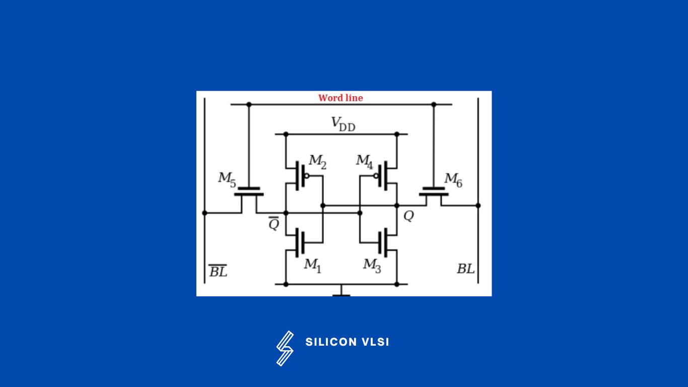
In SRAM memory, a single cell stores 1 bit of data. This data bit is represented by two inverters connected to a central circuit. The two inverters can alternatively connect to the central circuit through latches, functioning similarly to relay switches.
A typical SRAM cell, often known as a 6T SRAM cell, consists of six MOSFETs. Four transistors (M1, M2, M3, M4) make up two cross-coupled inverters (M1, M2, M3, M4). The following Circuit will perform Read and Write Operations in Memory Circuit. SRAM is more powerful than DRAM circuits.
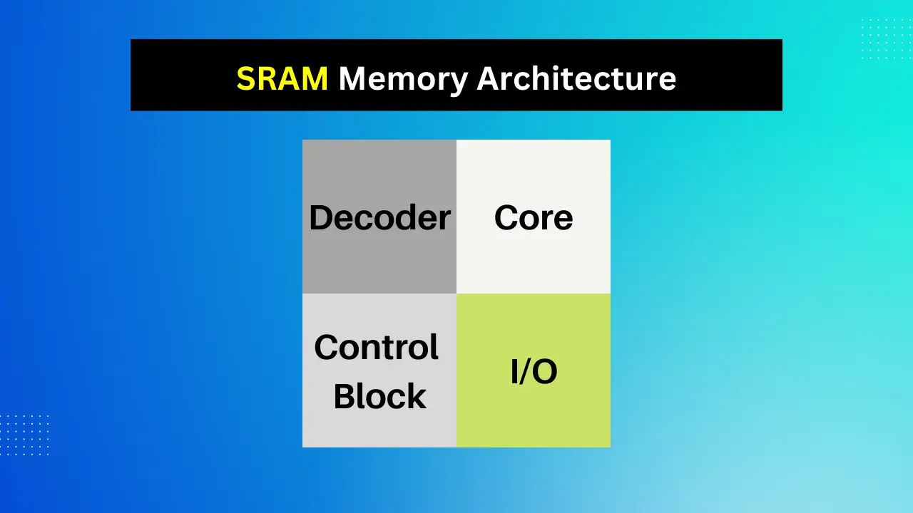
SRAM Memory Architecture
SRAM memory has Four main blocks, IO, Decoder, Array & Control Block.
Component of Core Block
- Memory cell (6T SRAM cell)
- Edge cell
- Corner cell
- Strap cell
- Filler Cell
Component of I/O Block
- Precharge#
- Multiplexer
- Sense Amplifier
- Write Driver
Component of Control Block
- CLK Gen
- Column Decoder
- Pre-decoder
Component of Decoder Block
- Decoder
- Selection Logic.