
The V-I characteristics curve of P-N junction diodes represents the relationship between voltage and current in the circuit. The voltage is plotted along the x-axis, while the current is plotted along the y-axis. The curve provides valuable insights into the operation of the diode and can be divided into three regions:
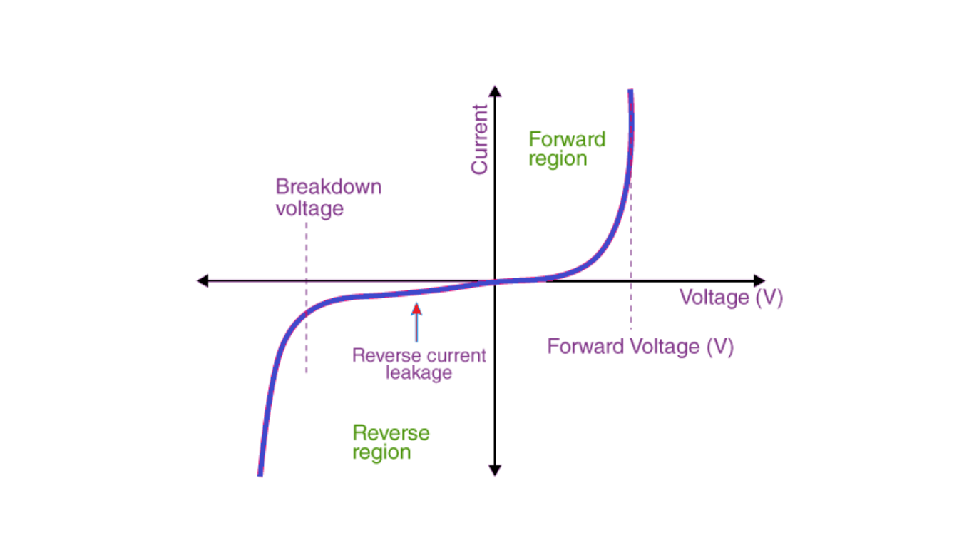
Forward Bias
In the forward bias condition, the p-type of the diode is connected to the positive terminal, and the n-type is connected to the negative terminal of the external voltage source. This configuration reduces the potential barrier. For silicone diodes, the potential barrier decreases when the voltage reaches 0.7 V, while for germanium diodes, it decreases at 0.3 V. As the potential barrier decreases, current starts to flow through the diode.
During forward bias, the current increases gradually, and the resulting curve is non-linear as the applied voltage surpasses the potential barrier. Once the diode overcomes the potential barrier, it behaves normally, and the curve exhibits a sharp rise as the external voltage increases, creating a linear relationship between voltage and current.
Reverse Bias
In the reverse bias condition, the p-type is connected to the negative terminal, and the n-type is connected to the positive terminal of the external voltage source. This setup increases the potential barrier, preventing significant current flow. However, a small reverse saturation current, resulting from the presence of minority carriers in the junction, does flow. When the applied voltage increases further, the minority charges gain more kinetic energy, impacting the majority charges. This stage is known as breakdown, and it can potentially damage or destroy the diode.
Zero Bias
In the zero bias condition, no external voltage is applied to the P-N junction diode. As a result, the potential barrier at the junction prevents the flow of current.
In summary, the V-I characteristics curve of a P-N junction diode provides valuable information about its behavior in different bias conditions, including zero bias, forward bias, and reverse bias. Understanding these characteristics is important for designing and utilizing diodes in electronic circuits.