

Voltage Transfer Characteristic (VTC): 7 Essential Concepts Explained
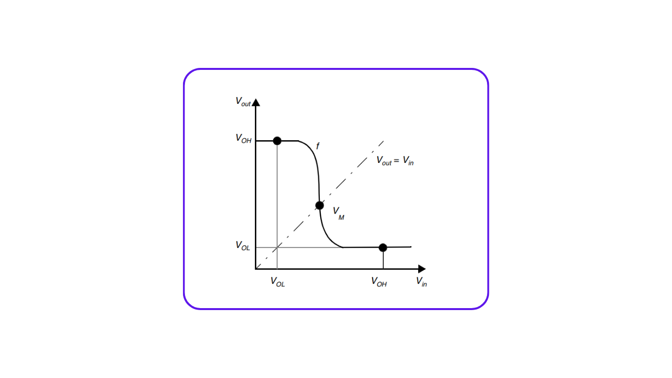
The Voltage Transfer Characteristic (VTC) is one of the most important concepts for understanding the electrical behavior of digital logic gates. It shows the relationship between the input voltage (Vin) and output voltage (Vout) of a gate.
For an inverting gate such as a CMOS inverter, the VTC shows how the output voltage changes as the input voltage increases from logic low toward logic high.
What Is a Voltage Transfer Characteristic?
A Voltage Transfer Characteristic (VTC) is a graph of:
Vout versus Vin
For a CMOS inverter:
- When Vin is low, the output is driven high.
- When Vin is high, the output is driven low.
- During the transition region, a small change in input voltage can produce a large change in output voltage.
The VTC therefore provides a visual representation of the DC voltage behavior of a digital gate.
For an ideal inverter, the transition from logic high to logic low would occur very sharply. In a practical CMOS inverter, the transition occurs over a finite voltage range.
Important Parameters of the VTC
Several important voltage levels can be obtained from the VTC:
- VOH — Output High Voltage
- VOL — Output Low Voltage
- VIH — Minimum Input High Voltage
- VIL — Maximum Input Low Voltage
- VM — Switching Threshold Voltage
- Noise Margins — NMH and NML
- Transition Width — Difference between VIH and VIL
These parameters help determine whether a digital circuit can reliably recognize logic 0 and logic 1.
1. VOH — Output High Voltage
VOH is the minimum guaranteed output voltage recognized as a logic-high output under specified conditions.
For a CMOS gate, VOH is typically close to the positive supply voltage when the output is logically high.
For example, in a circuit operating from a supply of 1.2 V, the output-high voltage may be close to 1.2 V, depending on the load and operating conditions.
2. VOL — Output Low Voltage
VOL is the maximum guaranteed output voltage recognized as a logic-low output.
For a CMOS gate, VOL is normally close to ground when the output is logically low.
Therefore, the practical output voltage ranges can be represented approximately as:
Logic 0 → 0 to VOL
Logic 1 → VOH to VDD
The exact specifications depend on the technology and operating conditions.
3. VM — Switching Threshold Voltage
The switching threshold voltage (VM) is an important point on the VTC of an inverter.
It is commonly defined as the point where:
Vin = Vout
Therefore, on a VTC plot, VM can be found where the inverter characteristic intersects the line:
Vout = Vin
At this point, the pull-up and pull-down behavior of the inverter is balanced according to the relevant DC operating condition.
VM is particularly useful when analyzing:
- CMOS inverter switching behavior
- Noise margins
- Inverter sizing
- Cascaded logic
- Circuits involving feedback
VM should not be confused with the MOSFET threshold voltage (VTH). They are different quantities.
4. VIL — Input Low Voltage
VIL is the highest input voltage that is guaranteed to be interpreted as a valid logic-low input.
For an inverter VTC, VIL is commonly identified at the point where the magnitude of the voltage gain reaches one:
dVout/dVin = −1
or equivalently:
|dVout/dVin| = 1
The region below VIL corresponds to the valid input-low region.
5. VIH — Input High Voltage
VIH is the lowest input voltage that is guaranteed to be interpreted as a valid logic-high input.
Similar to VIL, VIH is commonly obtained from the VTC at the point where:
dVout/dVin = −1
with the relevant intersection occurring on the high-input side of the transition region.
Therefore:
VIL < Vin < VIH
defines the transition or undefined region.
What Is the Undefined Region?
The voltage range between VIL and VIH is commonly called the undefined region or transition region.
It can be represented as:
VIL < Vin < VIH
A steady-state digital signal should normally not remain in this region.
Why?
Because in this region:
- The gate is transitioning between logic states.
- The output can be highly sensitive to small input changes.
- The noise margin is not guaranteed.
- The circuit may consume more short-circuit power during transitions.
- In some sequential situations, slow or noisy transitions can contribute to unreliable behavior.
Therefore, digital signals should ideally settle into the valid logic-low or logic-high regions.
Transition Width
The width of the transition region can be expressed as:
Transition Width = VIH − VIL
A smaller transition width generally indicates a sharper switching characteristic.
For a well-designed digital inverter, the VTC should have a relatively steep transition around the switching point.
Why Is the VTC Important?
The VTC provides important information about the DC characteristics and noise tolerance of a logic gate.
It helps designers determine:
Logic Voltage Levels
The VTC shows the relationship between input and output voltage and helps identify the valid logic regions.
Switching Behavior
The steep portion of the VTC shows where the inverter changes from one logic state to the other.
Noise Margins
The VTC can be used to determine how much unwanted voltage disturbance a circuit can tolerate without incorrectly interpreting a logic value.
Switching Threshold
VM provides information about the approximate switching point of the inverter.
Gate Quality
A sharp and appropriately positioned transition is generally desirable for reliable digital logic operation.
Noise Margin From the VTC
One of the most important applications of the VTC is determining noise margins.
The high-level noise margin is:
NMH = VOH − VIH
The low-level noise margin is:
NML = VIL − VOL
These values indicate how much noise can be tolerated while still maintaining valid logic levels.
For example, if:
- VOH = 1.0 V
- VIH = 0.7 V
then:
NMH = 1.0 − 0.7 = 0.3 V
Similarly, if:
- VIL = 0.3 V
- VOL = 0.1 V
then:
NML = 0.3 − 0.1 = 0.2 V
Higher noise margins generally provide better immunity to unwanted voltage disturbances.
VTC of a CMOS Inverter
A CMOS inverter consists of:
- One PMOS transistor
- One NMOS transistor
The two transistors form complementary pull-up and pull-down networks.
When Vin is Low
The PMOS is ON and the NMOS is OFF.
Therefore, the output is pulled toward:
VDD
So:
Vin = 0 → Vout ≈ VDD
When Vin is High
The PMOS is OFF and the NMOS is ON.
Therefore, the output is pulled toward:
GND
So:
Vin = 1 → Vout ≈ 0
During the Transition
As Vin moves through the transition region, both transistors can conduct simultaneously.
The output voltage changes rapidly from a high level toward a low level.
This creates the steep portion of the VTC.
VTC Regions of a CMOS Inverter
The inverter VTC can be understood through several operating regions:
| Input Region | PMOS | NMOS | Output Behavior |
|---|---|---|---|
| Low Vin | ON | OFF | Vout ≈ VDD |
| Increasing Vin | ON | Begins conducting | Vout starts decreasing |
| Transition region | Both conduct | Both conduct | Vout changes rapidly |
| High Vin | OFF | ON | Vout ≈ 0 |
The exact transistor operating regions depend on the input voltage and transistor parameters.
VTC and Voltage Gain
The voltage gain of an inverter is:
Av = dVout / dVin
Because a CMOS inverter is an inverting circuit, its gain is negative in the transition region.
Therefore:
Av < 0
At the points used to define VIL and VIH:
Av = −1
or, in terms of magnitude:
|Av| = 1
The steepness of the VTC is therefore directly related to the inverter’s voltage gain.
VTC and CMOS Inverter Sizing
The relative strength of the PMOS and NMOS transistors influences the VTC.
Changing transistor dimensions can shift the switching threshold and alter the shape of the VTC.
For example:
- Stronger NMOS → switching point can shift toward a lower input voltage.
- Stronger PMOS → switching point can shift toward a higher input voltage.
The exact shift depends on transistor parameters, supply voltage, sizing, process technology, and operating conditions.
This is why transistor sizing is important when designing CMOS logic gates.
VTC vs Logic Thresholds
It is important to distinguish these terms:
| Parameter | Meaning |
|---|---|
| VOH | Guaranteed output-high voltage |
| VOL | Guaranteed output-low voltage |
| VIH | Minimum guaranteed input-high voltage |
| VIL | Maximum guaranteed input-low voltage |
| VM | Inverter switching threshold where Vin = Vout |
| VTH | MOSFET transistor threshold voltage |
| NMH | High-level noise margin |
| NML | Low-level noise margin |
One common mistake is assuming VM and VTH are the same. They are not.
Why Should a Signal Avoid the Undefined Region?
A digital circuit is designed to interpret signals as either logic 0 or logic 1.
When an input remains between VIL and VIH, the circuit is operating in a region where the logic state is not guaranteed.
This can cause:
- Uncertain logic interpretation
- Increased sensitivity to noise
- Increased short-circuit current during transitions
- Timing problems when signals transition slowly
- Potential reliability issues in sequential circuits
Therefore, a clean digital signal should transition through this region and settle into a valid logic level.
VTC in VLSI Design
VTC analysis is especially important during CMOS design because it helps designers evaluate:
- Logic-level compatibility
- Noise margins
- Switching threshold
- Inverter sizing
- Process effects
- Supply-voltage effects
- Temperature effects
- PVT variation
- Overall robustness
A VTC is therefore more than just an input-output graph. It provides valuable information about the electrical quality of a digital logic gate.
Frequently Asked Questions
What is VTC in CMOS?
VTC stands for Voltage Transfer Characteristic. It represents the relationship between the output voltage and input voltage of a CMOS gate, commonly a CMOS inverter.
What does the VTC graph show?
The VTC graph shows how Vout changes as Vin changes. It can be used to identify VOH, VOL, VIL, VIH, VM, and noise margins.
What is VM in a CMOS inverter?
VM is the inverter’s switching threshold, commonly defined at the point where:
Vin = Vout
It is different from the MOSFET threshold voltage VTH.
What are VIH and VIL?
VIL is the maximum input voltage guaranteed to represent logic low, while VIH is the minimum input voltage guaranteed to represent logic high.
What is the undefined region?
The undefined region is the input-voltage range between:
VIL and VIH
A steady-state digital signal should not remain in this region.
How is noise margin calculated?
The common expressions are:
NMH = VOH − VIH
NML = VIL − VOL
Why is VTC important in VLSI?
VTC analysis helps designers evaluate switching behavior, logic levels, noise margins, sizing, and the robustness of CMOS logic circuits.