What is Routing in VLSI Physical Design? Process and Importance
In VLSI Physical Design, routing refers to the process of creating electrical connections between different components, such as standard cells, macros, and I/O pins, on a semiconductor chip. After placement is completed, routing defines the exact paths for metal wires that carry signals and power across the chip. Proper routing ensures signal integrity, minimizes delays, and optimizes chip performance. It is a critical step in the physical design flow, directly impacting the functionality, timing, and manufacturability of integrated circuits.

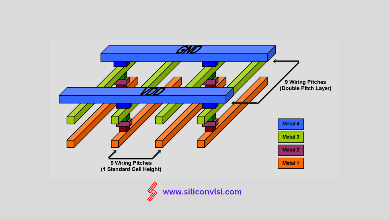
When we talk about routing in VLSI, we’re referring to the process of creating physical connections between signal pins using metal layers. This step is crucial because it follows Clock Tree Synthesis (CTS) and optimization, helping us determine the exact pathways for interconnecting standard cells, macros, and I/O pins. During the layout process, we establish electrical connections using metals and vias, which are derived from the logical connections in the netlist. Essentially, we convert logical connectivity into tangible physical connections in the design.
CTS encompasses information about all the cells, blockages, clock trees, buffers, inverters, and I/O pins incorporated into the design. The Routing program utilizes this data to establish all the required connections defined in the netlist, ensuring the absence of any Design Rule Check (DRC) violations. By making these connections, the tool ensures that:
- The design is completely routed.
- Congestion hotspots are either absent or minimized.
- Timing DRCs (Design Rule Checks) and Quality of Results (QOR) are met.
- There are minimal violations of Layout versus Schematic (LVS) and Signal Integrity (SI).
The mechanism of routing in VLSI involves the establishment of specific pathways for interconnections, including regular cell and macro pins, block boundary pins, and chip boundary pads. The tool incorporates information about the precise placements of blocks, block pins, and I/O pads at the chip borders after placement and CTS. It also utilizes the logical connections defined by the netlist. The routing stage employs metal and vias to construct the necessary electrical connections in the layout. Furthermore, the program relies on “Design Rules Checks (DRC)” to ensure proper linkages.
The steps involved in routing in VLSI are as follows
Global Route: The global route assigns nets to specific metal layers and global routing cells. The objective is to avoid congested global cells while minimizing diversions. Global routes also steer clear of pre-routed P/G (Power/Ground) connections, placement issues, and routing bottlenecks.
Track Assignment (TA): This step allocates each net to a specific track and lays down the actual metal traces. It aims to create long, straight lines to minimize the number of vias. Physical DRC is not taken into account at this stage.
Detail Routing: Detail routing addresses any DRC violations that arise after track assignment. It uses small regions (SBoxes) of a fixed size to repair these violations. Detail routing progresses through the entire design, box by box until the routing process is complete. It also incorporates timing-driven routing techniques.
In conclusion, if you are interested in learning more about VLSI design, you can enroll in one of the online VLSI courses offered by Chipedge, a leading VLSI training institute in Bangalore. They provide a wide range of courses, including design verification courses and RTL design courses. For further information, please feel free to contact them.