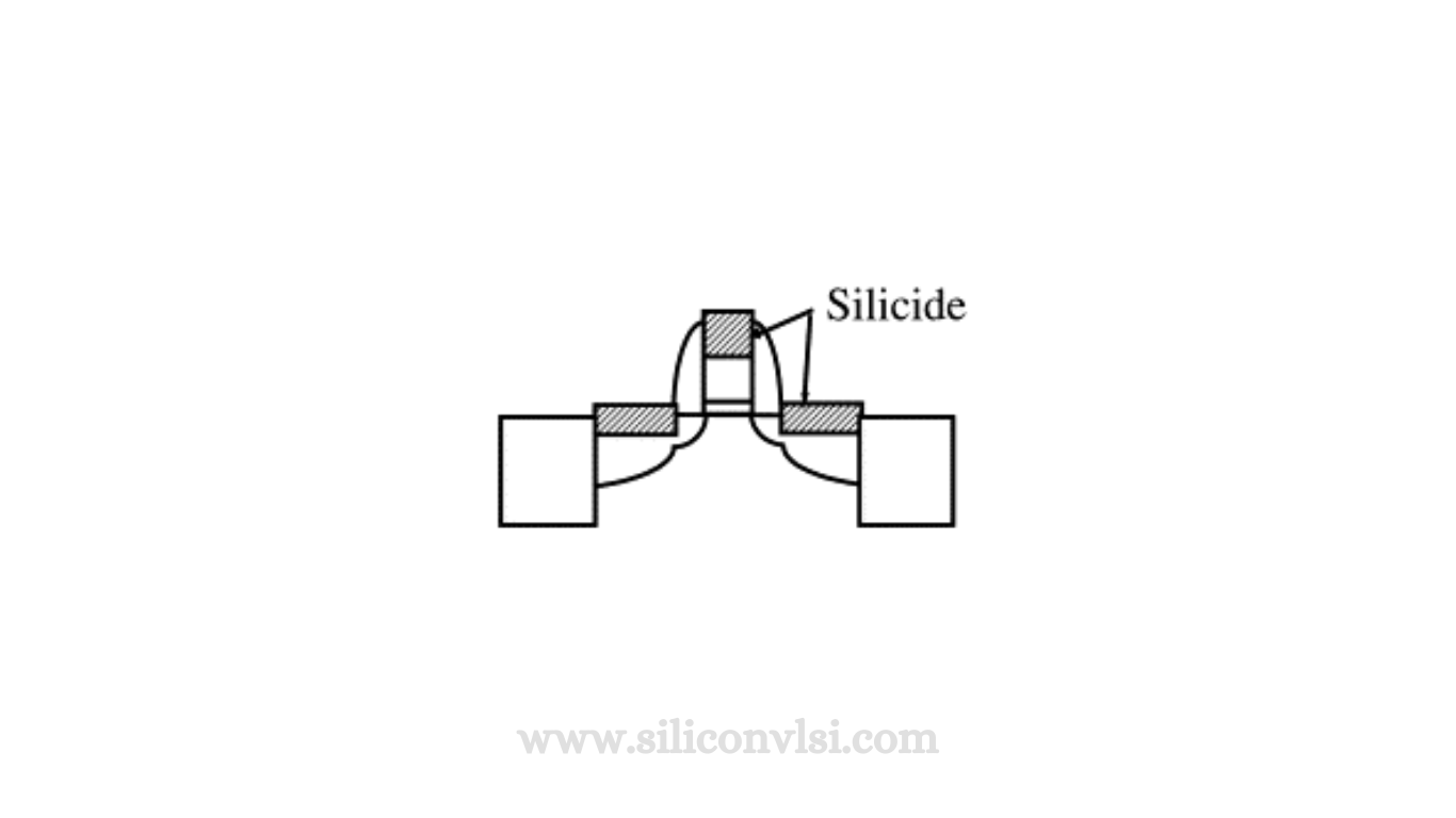
Silicidation Process
The modification in semiconductor metallization involving the addition of silicide is a crucial enhancement to the standard metallization flow. Elemental silicon reacts with metals such as platinum, palladium, titanium, and nickel to form silicides with definite compositions. Silicides offer the advantage of forming both low-resistance Ohmic contacts and, in certain cases, stable rectifying Schottky barriers. This not only improves contact resistance, addressing issues with barrier metal systems but also allows the cost-free formation of Schottky diodes. Silicides exhibit much lower resistivities than heavily doped silicon, making them useful for reducing the resistance of selected silicon regions.

The deposition process of a Platinum silicide layer
The deposition process of a platinum silicide layer involves depositing a thin film of platinum metal across the entire wafer, followed by heating to induce a reaction with silicon, forming platinum silicide. Unreacted platinum can then be removed, leaving silicide contact openings and exposed polysilicon. Additional masking steps can be employed to select specific regions for silicidation. Processes involving clad poly often use a silicide block mask to fabricate polysilicon resistors, preventing silicidation from turning all polysilicon into low-resistance material.
A typical silicided metal system comprises a lowermost layer of platinum silicide, an intermediate layer of refractory barrier metal, and a topmost layer of copper-doped aluminum. This combination offers low electrical resistance, high electromagnetic immunity, stable contact resistance, and precisely controlled alloying depths. While the three-layer system may be costlier than simple aluminum alloy metallization, the substantial performance benefits make it a preferred choice in semiconductor fabrication.