Close Menu
  • Analog Design
    • Latest Analog Layout Interview Questions (2025)
  • Digital Design
    • Digital Electronics Interview Question(2025)
    • Top VLSI Interview Questions
  • Physical Design
    • Physical Design Interview Questions for VLSI Engineers
  • Verilog
    • Verilog Interview Questions(2024)
  • Forum
Facebook Instagram YouTube LinkedIn WhatsApp
SiliconvlsiSiliconvlsi
Forum Questions Register in Forum Login in Forum
Facebook Instagram YouTube LinkedIn WhatsApp
  • Analog Design
    • Latest Analog Layout Interview Questions (2025)
  • Digital Design
    • Digital Electronics Interview Question(2025)
    • Top VLSI Interview Questions
  • Physical Design
    • Physical Design Interview Questions for VLSI Engineers
  • Verilog
    • Verilog Interview Questions(2024)
  • Forum
SiliconvlsiSiliconvlsi
Home»VLSI Design»What is the exact difference between port and pin in VLSI ?
VLSI Design

What is the exact difference between port and pin in VLSI ?

siliconvlsiBy siliconvlsiJanuary 9, 2022Updated:May 12, 2024No Comments1 Min Read
Facebook Pinterest LinkedIn Email WhatsApp
Share
Facebook Twitter LinkedIn Pinterest Email

The following figure may get a clear idea about which is the pin and which is the port.

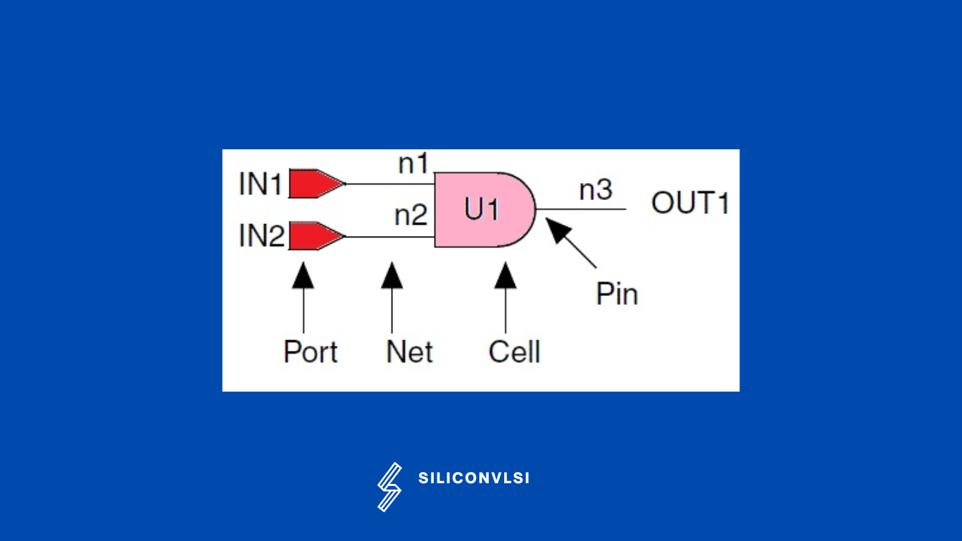
A pin is a physical connection for a single net.

A port is a group of pins representing a standard interface.

In the physical world, a port is usually more than one pin

Nets are used for internal Interconnection

In VLSI physical design, ports and pins both serve as interfaces between the chip and the outside world, but they have distinct roles.

A port is a group of related signals grouped together for convenience. Ports typically represent the inputs and outputs of a specific module or block within the chip.

In contrast, a pin is a physical connection point on the chip where an external signal can be linked. Pins represent the actual physical connections to the chip, such as input/output pads or bonding pads.

In summary, ports organize logical signal groupings within the chip, while pins denote the physical connection points on the chip.

Share. Facebook Twitter Pinterest LinkedIn Tumblr Email

Related Posts

How Shielding Avoids Crosstalk Problem? What Exactly Happens There?

September 22, 2024

Navigating the Challenges of Gate Dielectric Scaling in MOS Transistors

August 1, 2024

Challenges in Modern SoC Design Verification

April 20, 2024
Leave A Reply Cancel Reply

Facebook X (Twitter) Instagram Pinterest Vimeo YouTube
  • About Us
  • Contact Us
  • Privacy Policy
© 2025 Siliconvlsi.

Type above and press Enter to search. Press Esc to cancel.