Close Menu
  • Analog Design
    • Latest Analog Layout Interview Questions (2025)
  • Digital Design
    • Digital Electronics Interview Question(2025)
    • Top VLSI Interview Questions
  • Physical Design
    • Physical Design Interview Questions for VLSI Engineers
  • Verilog
    • Verilog Interview Questions(2024)
  • Forum
Facebook Instagram YouTube LinkedIn WhatsApp
SiliconvlsiSiliconvlsi
Ask Questions Register in Forum Login in Forum
Facebook Instagram YouTube LinkedIn WhatsApp
  • Analog Design
    • Latest Analog Layout Interview Questions (2025)
  • Digital Design
    • Digital Electronics Interview Question(2025)
    • Top VLSI Interview Questions
  • Physical Design
    • Physical Design Interview Questions for VLSI Engineers
  • Verilog
    • Verilog Interview Questions(2024)
  • Forum
SiliconvlsiSiliconvlsi
Home»Digital Design»Why NMOS pass strong 0 and weak 1
Digital Design

Why NMOS pass strong 0 and weak 1

siliconvlsiBy siliconvlsiOctober 2, 2022Updated:June 8, 2025No Comments2 Mins Read
Facebook Pinterest LinkedIn Email WhatsApp
Share
Facebook Twitter LinkedIn Pinterest Email

Why NMOS pass strong 0 and weak 1

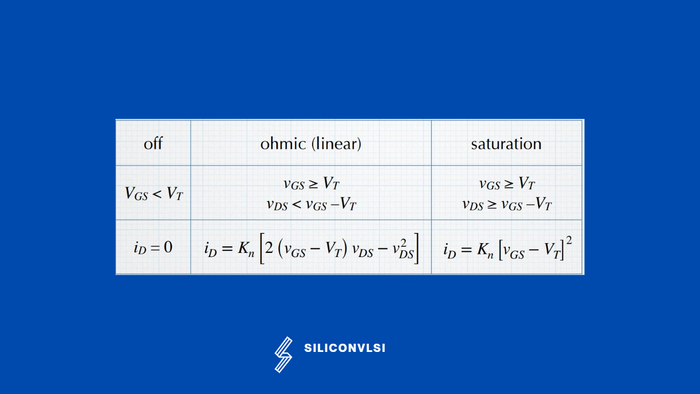
We all know that when Vgs > Vt, at that time only Nmos will turn on.

NMOS Current Equation:

NMOS Current Equation

Now to understand  NMOS pass strong 0 and weak 1, let’s take one example. Suppose we have one NMOS. As shown in the following figure, let’s take Vdd=1v, Vgs=1v, and Threshold voltage(Vt) = 0.2v. And Initially, Capacitor(Vcc) is 0v.


After Some time, lets assume that capacitor Vcc, Charged by 0.2v, so Vgs = Vg – Vs = 1 – 0.2 = 0.8 > 0.2(vt). So node Vcc charged by 0.2v and still Vgs is greater than Vt. So still current will flow from the drain to the source.


After Some time, that capacitor Vcc is charged by 0.6v, so Vgs = Vg – Vs = 1 – 0.6= 0.4 > 0.2(vt). So node Vcc charged by 0.6v and still Vgs is greater than Vt. So still current will flow from the drain to the source.


After Some time,that capacitor Vcc, charged by 0.8v, so Vgs = Vg – Vs = 1 – 0.8= 0.2 = 0.2(vt). So node Vcc charged by 0.8v and still Vgs is equal to Vt. So still current will flow from the drain to the source.

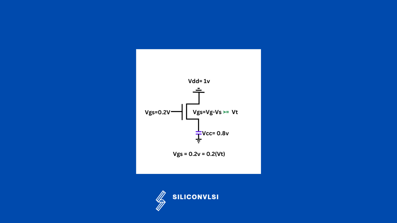
Now As soon As Vcc becomes 0.8v, after that, it will not charge further because Vgs > Vt, the condition is not satisfying, so at 0.8v only, NMOS will pass, and after that, it will stop charging that capacitor. Based on the above explanation, we can say that NMOS is Weak to pass 1, which means NMOS can not fully charge the capacitor. It will charge up to  Vcc = Vdd – Vt.

NMOS Pass Characteristics


Please comment below if You like this article.

Share. Facebook Twitter Pinterest LinkedIn Tumblr Email

Related Posts

Understanding the Difference Between RAM Bandwidth and Clock Speed

December 1, 2024

Why is Frequency Planning so important in Module Design?

September 2, 2024

How Are Electrostatic Discharge (ESD) Protection and Latch-Up Related to Each Other?

July 20, 2024
Leave A Reply Cancel Reply

Facebook X (Twitter) Instagram Pinterest Vimeo YouTube
  • About Us
  • Contact Us
  • Privacy Policy
© 2025 Siliconvlsi.

Type above and press Enter to search. Press Esc to cancel.