

Why PMOS pass strong 1 and weak 0
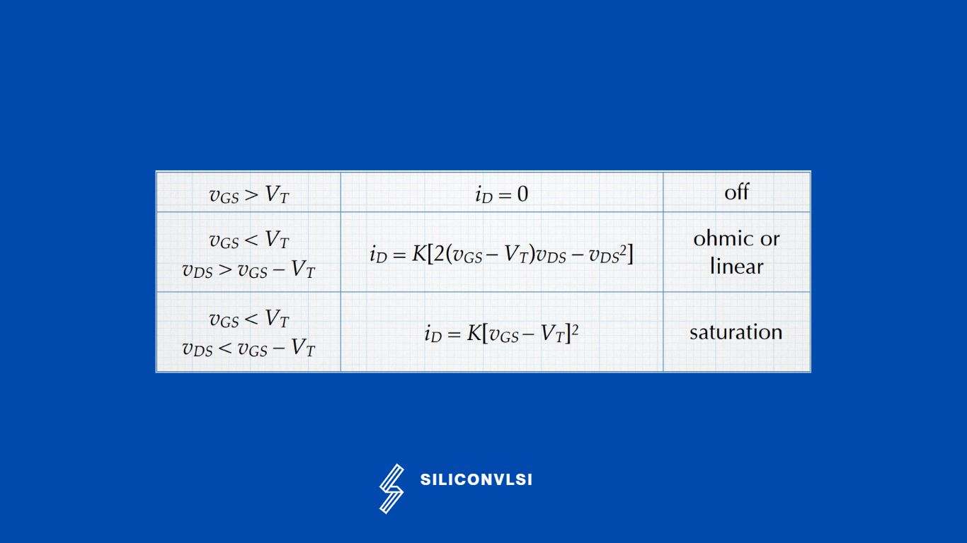
The current equation for PMOS is the following, for PMOS to turn on, Vgs should be less than Vt.
The current equation for PMOS
Now to understand PMOS pass strong 1 and weak 0, let’s take one example. Suppose we have one PMOS. As shown in the following figure, let’s take Vcc =1v, Vg = 0, and Threshold voltage(Vt) = – 0.2v. And Initially, Capacitor(Vcc) is 1v. And drain terminal is tied to ground

After some time, As shown in the following figure, after discharge, Vcc node is 0.8v, Vg = 0 and Threshold voltage(Vt) = – 0.2v.
So Vgs = Vg – Vs = 0 – 0.8 = -0.8 < -0.2. This means still Vgs < Vt condition is satisfying.

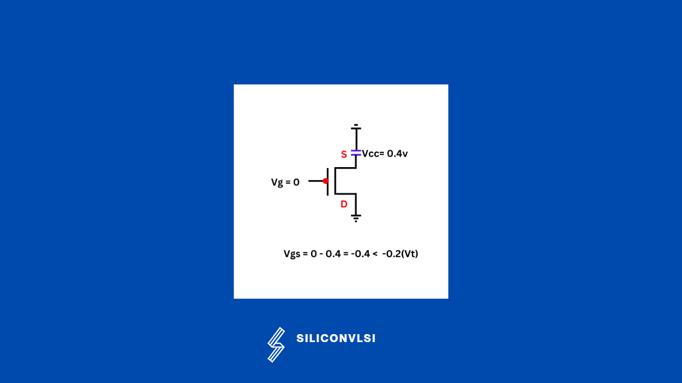
After some time, As shown in the following figure, after some more discharge, Vcc node is 0.4v, Vg = 0 and Threshold voltage(Vt) = – 0.2v. So Vgs = Vg – Vs = 0 – 0.4= -0.4< -0.2. This means still Vgs < Vt condition is satisfying.
After some time, As shown in the following figure, after some more discharge, Vcc node is 0.2v, Vg = 0 and Threshold voltage(Vt) = – 0.2v. So Vgs = Vg – Vs = 0 – 0.2= -0.2 = -0.2. This means still Vgs < Vt condition is satisfying.
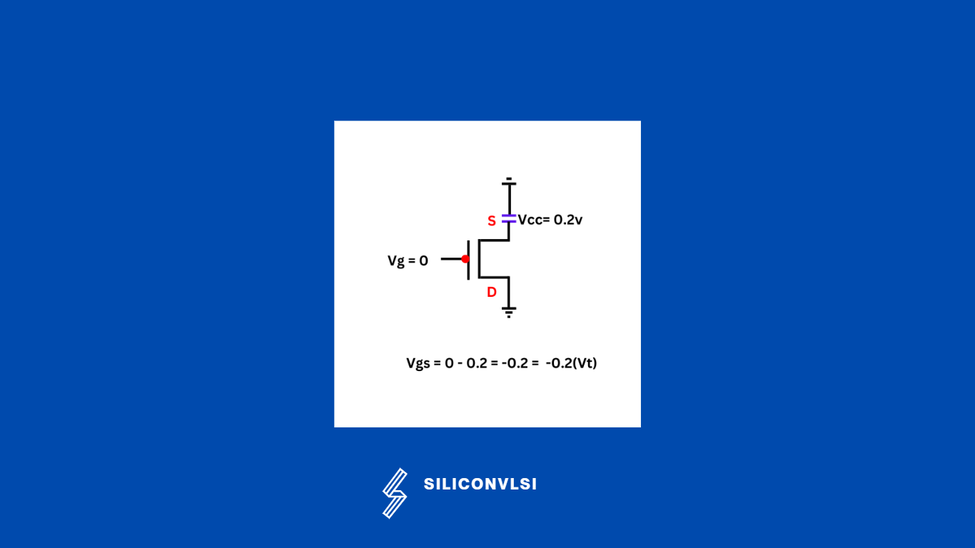
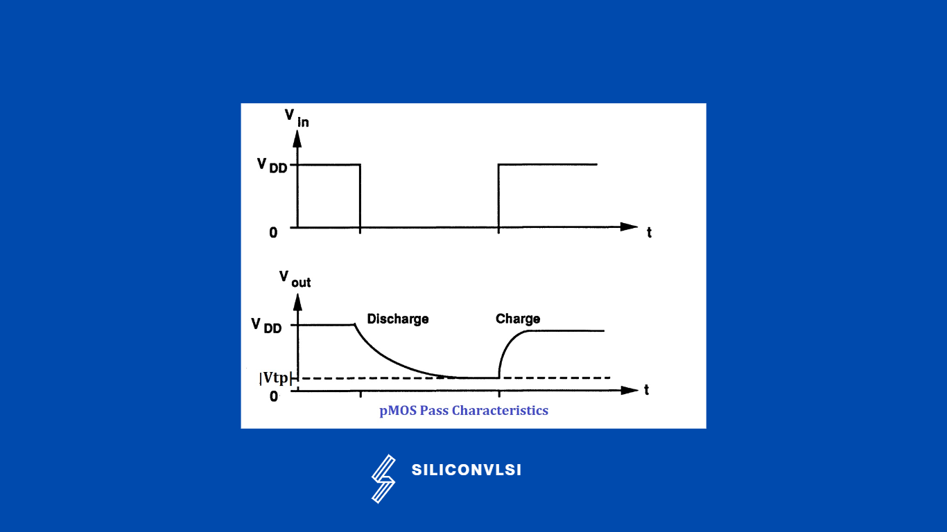
Now we reach a critical point of PMOS, now after that, this Vcc cap will not discharge further because Vg -Vs < Vt condition will no more satisfying. So based on the above example, we can say that PMOS passes weak Zero. This means in the above example, the capacitor will not be discharged fully.
pMOS Pass Characteristics
What is the meaning of strong 1 and strong 0?
In digital circuitry, when we refer to a “strong 1” or a “strong 0,” we mean that the output signal is capable of strongly driving either a high voltage (Vdd) or a low voltage (ground, GND), respectively.
For an NMOS (N-type Metal-Oxide-Semiconductor) transistor to be turned ON and allow the passage of a high signal (logic 1), its gate should be supplied with a voltage equal to Vdd.
Conversely, for a PMOS (P-type Metal-Oxide-Semiconductor) transistor to be turned ON and allow the passage of a low signal (logic 0), its gate should be connected to the ground (GND).
This distinction ensures that the transistors in the circuit behave appropriately to produce the desired logic levels at the output.
Common Mistakes to Avoid
Mistake 1: Saying PMOS Passes Weak 1
This is incorrect for the idealized pass-transistor concept.
The standard rule is:
PMOS passes strong 1 and weak 0.
Mistake 2: Saying the PMOS Immediately Stops at 0V
The PMOS does not simply stop conducting because the output becomes low.
Its drive decreases as the source/output voltage falls.
The important condition is:
VSG approaches |VTP|
At that point, normal channel conduction becomes very small.
Mistake 3: Assuming the Threshold Voltage Is Always Constant
The simple example normally assumes a constant threshold voltage.
In practical devices, body effect and other device effects can change the effective threshold.
Mistake 4: Thinking Strong Means “Higher Current”
Strong and weak logic levels primarily describe the voltage level that can be transferred or restored, not simply the magnitude of current.
Frequently Asked Questions
Why does PMOS pass strong 1 and weak 0?
A PMOS can pull an output close to VDD when passing HIGH because its VSGV_{SG} remains sufficient as the output rises. When passing LOW, the source voltage falls, reducing VSGV_{SG} until it approaches ∣VTP∣|VTP|, leaving a degraded LOW level.
What voltage does PMOS pass as a strong 1?
Ideally, a PMOS can pass a HIGH level close to VDD.
What voltage does PMOS pass as a weak 0?
In the simplified constant-threshold model, the output may stop around:
VOUT ≈ |VTP|
above ground.
Which transistor passes strong 0?
An NMOS passes a strong 0 and a weak 1.
Which transistor passes strong 1?
A PMOS passes a strong 1 and a weak 0.
How can both 0 and 1 be passed strongly?
A CMOS transmission gate, consisting of parallel NMOS and PMOS devices controlled by complementary signals, can transfer both logic levels effectively.
Does body effect affect PMOS pass behavior?
Yes. Body effect can change the effective threshold voltage and therefore change the actual voltage at which the PMOS stops conducting.
Key Takeaways
- A PMOS passes strong 1 and weak 0.
- A PMOS can transfer a HIGH level close to VDD.
- When transferring LOW, the source/output voltage falls.
- As the source voltage falls, VSG decreases.
- When VSGVSG approaches ∣VTP∣|VTP|, the PMOS approaches its turn-off condition.
- Therefore, the LOW output may remain approximately at ∣VTP∣|VTP| above ground in the simplified model.
- An NMOS exhibits the opposite behavior: strong 0 and weak 1.
- A transmission gate combines NMOS and PMOS to transfer both logic levels effectively.
- Body effect and other nonidealities can change the exact voltage in a practical circuit.
- This concept is important for CMOS pass-transistor logic, multiplexers, transmission gates, dynamic circuits, and VLSI design.