Close Menu
  • Analog Design
    • Latest Analog Layout Interview Questions (2025)
  • Digital Design
    • Digital Electronics Interview Question(2025)
    • Top VLSI Interview Questions
  • Physical Design
    • Physical Design Interview Questions for VLSI Engineers
  • Verilog
    • Verilog Interview Questions(2024)
  • Forum
Facebook Instagram YouTube LinkedIn WhatsApp
SiliconvlsiSiliconvlsi
Ask Questions Register in Forum Login in Forum
Facebook Instagram YouTube LinkedIn WhatsApp
  • Analog Design
    • Latest Analog Layout Interview Questions (2025)
  • Digital Design
    • Digital Electronics Interview Question(2025)
    • Top VLSI Interview Questions
  • Physical Design
    • Physical Design Interview Questions for VLSI Engineers
  • Verilog
    • Verilog Interview Questions(2024)
  • Forum
SiliconvlsiSiliconvlsi
Home»Digital Design»Application of pn junction Diode
Digital Design

Application of pn junction Diode

siliconvlsiBy siliconvlsiJune 26, 2023Updated:June 17, 2025No Comments2 Mins Read
Facebook Pinterest LinkedIn Email WhatsApp
Share
Facebook Twitter LinkedIn Pinterest Email

What is the use of a PN junction diode?

The application of a PN junction diode is when you forward-bias the PN junction diode; you use it in LED lighting. You apply it as a rectifier in many electric circuits, and you utilize it as a voltage-controlled oscillator in varactors. A P-N junction is like a border between two different types of materials inside a semiconductor. These materials are called p-type and n-type.

Application of pn junction diode

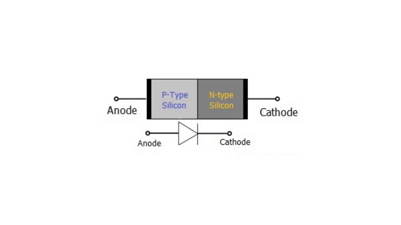
To create a P-N junction in a semiconductor, we use a process called doping. On one side of the semiconductor, called the p-side or positive side, there are extra holes. On the other side, called the n-side or negative side, there are extra electrons. Doping is explained in more detail in the next part.

Application of pn junction Diode are following

  • In computer digital logic circuits, diodes are utilized as switches.
  • It is used as a switch in digital logic designs.
  • It is used in detector and demodulator circuits.
  • It is used in clamping circuits in TV receivers as well as voltage multipliers.
  • It is used as a rectifier in DC power supply manufacturing.
  • When using optical communications, laser diodes are employed.
  • Digital displays use Light light-emitting diodes (LEDs).

How You Form a P–N Junction with Doping

You know that joining different semiconductor materials creates grain boundaries that scatter electrons and holes, hindering their flow. To prevent this, you use doping. For instance, take a thin p-type silicon sheet and introduce a small amount of pentavalent impurity—you’ll convert part of it into n-type silicon. You then have adjacent p- and n-regions forming a p–n junction. After formation, you rely on diffusion and drift to drive carrier movement.

solar cell rectifier
Share. Facebook Twitter Pinterest LinkedIn Tumblr Email

Related Posts

Difference Between Clipper and Clamper

June 22, 2025

Understanding the Difference Between RAM Bandwidth and Clock Speed

December 1, 2024

Why is Frequency Planning so important in Module Design?

September 2, 2024
Leave A Reply Cancel Reply

Facebook X (Twitter) Instagram Pinterest Vimeo YouTube
  • About Us
  • Contact Us
  • Privacy Policy
© 2025 Siliconvlsi.

Type above and press Enter to search. Press Esc to cancel.