
Carrier Concentration in Semiconductor
Carrier concentration in semiconductors is all about how many free charge carriers—like electrons in the conduction band and holes in the valence band—are available in a material. When you and I explore how semiconductors work, it’s clear that these carriers are the ones actually responsible for carrying electric current. The more carriers we have, the better the conductivity.
Types of Carriers
There are two main types of carriers in semiconductor materials: majority carriers and minority carriers. The majority of carriers are the dominant charged particles, either electrons or holes, which exist in larger quantities. On the other hand, minority carriers are present in smaller amounts compared to the majority carriers.
Factors Affecting Carrier Concentration
Various factors have an impact on the concentration of carriers in a semiconductor material. One significant factor is doping, which involves deliberately introducing impurities into the material to modify its electrical properties. Doping can greatly increase the carrier concentration and control how conductive the material is.
When the temperature rises, the number of charge carriers generated due to thermal energy increases, resulting in a higher carrier concentration. Conversely, at lower temperatures, the carrier concentration decreases.
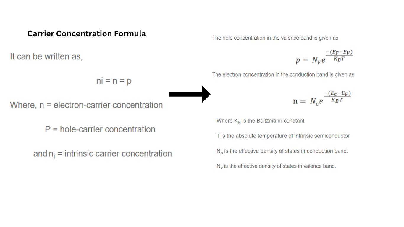
Carrier Concentration Formula
Fermi Level in Semiconductors: What You and I Need to Know
The Fermi level plays a key role when we try to understand how charge carriers behave in semiconductors. It’s the energy level where there’s a 50% chance of finding an electron. As you and I explore semiconductor physics, we see that the Fermi level isn’t fixed—it shifts depending on temperature and the number of charge carriers.
In intrinsic semiconductors, the Fermi level usually sits near the center of the band gap. But if we’re working with n-type materials, it moves closer to the conduction band. For p-type semiconductors, it shifts toward the valence band. This movement is influenced by both temperature and doping levels. So, when you’re designing or analyzing semiconductor devices, keeping an eye on the Fermi level gives you valuable insight into how the material will perform electrically.