

Complementary Metal-Oxide-Semiconductor (CMOS): 7 Essential Concepts You Should Know
Complementary Metal-Oxide-Semiconductor (CMOS) is one of the most important technologies used to build modern integrated circuits (ICs). CMOS uses complementary PMOS and NMOS transistors to implement digital logic with low static power consumption.
CMOS technology is widely used in processors, memory, microcontrollers, smartphones, ASICs, and other VLSI circuits. Its combination of low power consumption, high integration density, and good noise margins has made it the dominant technology for modern digital ICs.
What Is CMOS?
CMOS stands for Complementary Metal-Oxide-Semiconductor.
The word complementary refers to the use of both NMOS and PMOS transistors in a circuit. In a typical CMOS logic gate, these two transistor networks work in a complementary manner:
- The PMOS network pulls the output toward the supply voltage.
- The NMOS network pulls the output toward ground.
- Ideally, one network is conducting while the other is off in a stable logic state.
This structure helps CMOS achieve very low static power consumption.
Why Is CMOS Important in VLSI?
CMOS technology is particularly important because it provides several advantages for highly integrated circuits.
Some major benefits include:
- Low static power consumption
- High integration density
- Good noise immunity
- High input impedance
- Wide range of available supply-voltage technologies
- Suitable for large-scale digital integration
- Compatibility with modern VLSI manufacturing
Because millions or billions of transistors can be integrated into modern chips, reducing power consumption at the transistor level is extremely important.
How Does CMOS Logic Work?
A simple CMOS inverter contains one PMOS and one NMOS transistor.
When the input is LOW:
- PMOS turns ON.
- NMOS turns OFF.
- Output becomes HIGH.
When the input is HIGH:
- PMOS turns OFF.
- NMOS turns ON.
- Output becomes LOW.
This complementary operation allows the CMOS inverter to provide a strong logic 0 and logic 1 while keeping static current low in the idealized steady state.
Advantages of CMOS Logic
CMOS has several important advantages over older logic technologies.
1. Low Power Consumption
One of the most important advantages of CMOS is its low static power consumption.
In a conventional CMOS gate, there is ideally no direct DC path from VDD to ground when the circuit is in a stable logic state.
However, real CMOS circuits consume power through:
- Dynamic switching
- Leakage currents
- Short-circuit current during transitions
Dynamic power can be approximated by:
Pdynamic ≈ α × C × VDD² × f
where:
- α = switching activity
- C = effective capacitance
- VDD = supply voltage
- f = switching frequency
This is one reason voltage scaling is an important low-power design technique.
2. High Input Impedance
MOSFET gates are insulated from the channel by the gate dielectric. As a result, CMOS inputs have very high DC input impedance.
This means a CMOS gate generally draws very little DC input current compared with many bipolar logic circuits.
3. Good Noise Immunity
CMOS logic generally provides good noise margins, allowing digital signals to tolerate a certain amount of unwanted voltage disturbance without being incorrectly interpreted.
The exact noise margin depends on the particular CMOS technology and voltage levels.
4. High Integration Density
CMOS technology supports the integration of very large numbers of transistors onto a single chip.
This makes it suitable for:
- CPUs
- GPUs
- SRAM
- Microcontrollers
- ASICs
- SoCs
- Digital signal processors
Modern semiconductor manufacturing has continued to improve transistor density and performance while reducing operating voltages.
5. Wide Range of Applications
CMOS technology is used in many areas of electronics, including:
- Digital logic
- Memory circuits
- Microprocessors
- Microcontrollers
- Mobile processors
- Communication ICs
- Image sensors
- Mixed-signal ICs
- Analog circuits
- VLSI systems
Disadvantages of CMOS Logic Gates
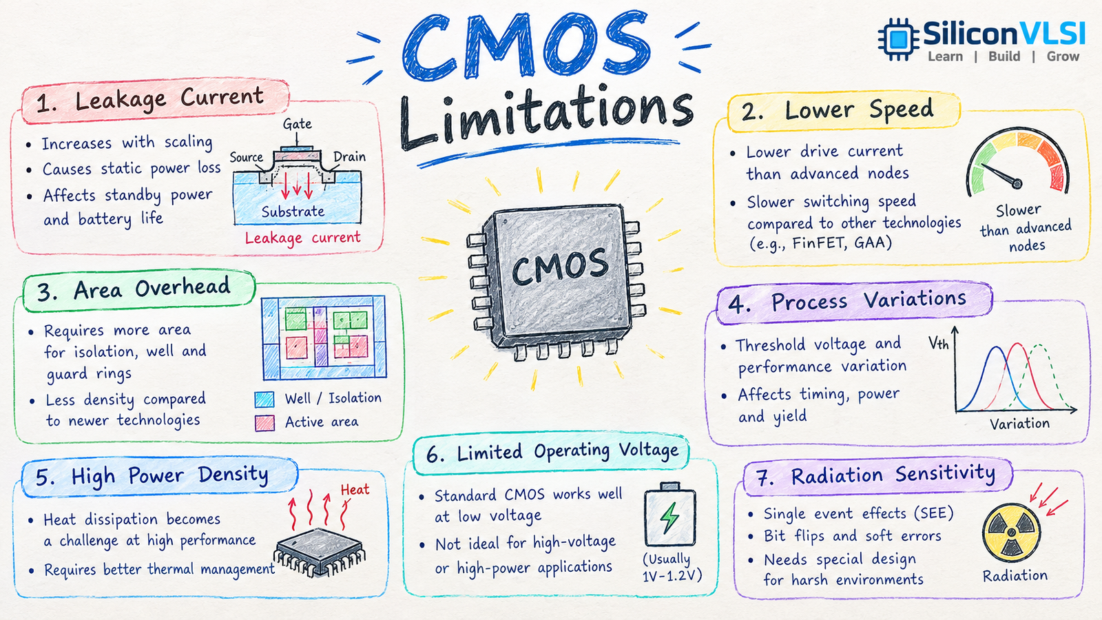
Although CMOS has many advantages, it also has limitations.
1. Dynamic Power Increases With Switching
CMOS has low static power, but dynamic power becomes significant when circuits switch frequently.
Higher switching activity, capacitance, supply voltage, or frequency can increase dynamic power.
Therefore, modern VLSI designers use techniques such as clock gating, power gating, voltage scaling, and capacitance reduction to control power consumption.
2. Leakage Current
As transistor dimensions have become smaller, leakage currents have become an important source of power consumption.
Major CMOS leakage mechanisms include:
- Subthreshold leakage
- Gate leakage
- Reverse-biased junction leakage
- Gate-induced drain leakage (GIDL)
Leakage becomes particularly important in highly scaled technologies and at elevated temperatures.
3. ESD Sensitivity
MOS structures can be sensitive to electrostatic discharge (ESD) because excessive voltage can damage thin gate dielectrics.
Modern CMOS ICs therefore include ESD protection structures at interfaces such as input/output pads.
4. Process Complexity
CMOS manufacturing requires multiple fabrication steps and carefully controlled process layers.
Modern CMOS processes may involve:
- Multiple lithography steps
- Well formation
- Isolation
- Source/drain formation
- Gate formation
- Multiple metal layers
- Contacts and vias
The exact process complexity depends strongly on the technology node and manufacturing platform.
5. Power and Performance Trade-Off
Reducing the supply voltage can significantly reduce dynamic power, but it can also reduce noise margins and transistor drive capability.
Therefore, CMOS designers must balance:
Power ↔ Performance ↔ Area ↔ Reliability
This is especially important in modern VLSI design.
CMOS vs NMOS
CMOS and NMOS are both MOS-based logic technologies, but their transistor usage is different.
| Feature | CMOS | NMOS |
|---|---|---|
| Transistors | PMOS + NMOS | Primarily NMOS logic network |
| Static Power | Very low in conventional CMOS | Generally higher |
| Noise Margin | Generally good | Typically lower than CMOS for comparable conditions |
| Power Efficiency | High | Lower |
| Integration | Very high | Historically important |
| Modern Use | Dominant digital IC technology | Mostly of historical/legacy importance |
The complementary use of PMOS and NMOS is a major reason CMOS can achieve low static power.
CMOS vs TTL
CMOS and TTL are different logic families.
| Feature | CMOS | TTL |
|---|---|---|
| Main transistor type | MOSFET | BJT |
| Static power | Generally low | Generally higher |
| Input impedance | High | Lower |
| Supply options | Many CMOS families support different voltage ranges | Traditional TTL is strongly associated with 5 V |
| Integration density | Very high | Lower than modern CMOS |
| Modern VLSI use | Dominant | Mainly legacy/specialized applications |
It is important not to say that TTL is always faster than CMOS. Switching performance depends on the specific logic family, process technology, load, and operating conditions. Modern CMOS technology can operate at very high speeds.
CMOS Technology in Modern VLSI
Modern CMOS technology has evolved considerably from the traditional planar MOSFET structure.
Depending on the process generation, semiconductor manufacturers may use structures such as:
- Planar MOSFETs
- FinFETs
- Gate-all-around (GAA) transistors
These structures are designed to improve transistor control and support continued scaling.
At the same time, advanced CMOS processes use increasingly sophisticated interconnect, isolation, power-delivery, and manufacturing techniques.
CMOS in Analog and Mixed-Signal Circuits
CMOS is not limited to digital logic.
CMOS technology is also widely used for analog and mixed-signal circuits such as:
- Operational amplifiers
- Current mirrors
- Comparators
- ADCs and DACs
- PLLs
- Voltage references
- Sensor interfaces
Analog CMOS design requires careful consideration of transistor matching, noise, parasitic capacitance, gain, output resistance, and layout.
Common CMOS Design Problems
Some important issues encountered in CMOS and VLSI design include:
- Leakage current
- IR drop
- Electromigration
- Crosstalk
- Signal integrity
- Process variation
- Device mismatch
- Latch-up
- ESD
- Timing violations
- Power consumption
Physical design techniques and proper circuit architecture are required to manage these effects.
Frequently Asked Questions
What does CMOS stand for?
CMOS stands for Complementary Metal-Oxide-Semiconductor.
Why is CMOS widely used in VLSI?
CMOS offers low static power consumption, high integration density, good noise margins, and excellent scalability, making it suitable for large digital integrated circuits.
What are the main disadvantages of CMOS?
Important limitations include leakage power, dynamic switching power, ESD sensitivity, manufacturing complexity, and power-performance trade-offs.
Is CMOS better than NMOS?
For most modern digital IC applications, CMOS is preferred because complementary PMOS and NMOS operation provides much lower static power consumption than traditional NMOS logic.
Is CMOS used only for digital circuits?
No. CMOS technology is also widely used for analog and mixed-signal circuits, including amplifiers, ADCs, DACs, PLLs, and sensor interfaces.
Why does CMOS consume low power?
In conventional CMOS logic, ideally one transistor network is OFF in a stable logic state, greatly reducing direct static current between the supply and ground. Real circuits still consume leakage and dynamic power.
Conclusion
Complementary Metal-Oxide-Semiconductor (CMOS) is a fundamental technology behind modern integrated circuits. Its complementary PMOS and NMOS structure provides low static power consumption, good noise margins, high input impedance, and high integration density.
Although CMOS has challenges such as leakage, dynamic power, ESD sensitivity, and increasing process complexity, continuous improvements in transistor structures and manufacturing have allowed CMOS technology to remain central to modern VLSI.
Understanding CMOS is therefore an essential starting point for learning digital logic, semiconductor devices, VLSI design, physical design, low-power design, and modern integrated circuits.