
What is latchup in CMOS and its prevention Techniques
“Latch-up is the state where a semiconductor undergoes a high-current state or low impedance path as a result of the interaction of PNP and NPN bipolar transistors. Latch-up is a phenomenon whereby Vdd and Vss in a CMOS device become structurally shorted due to the effect of noise or etc.”
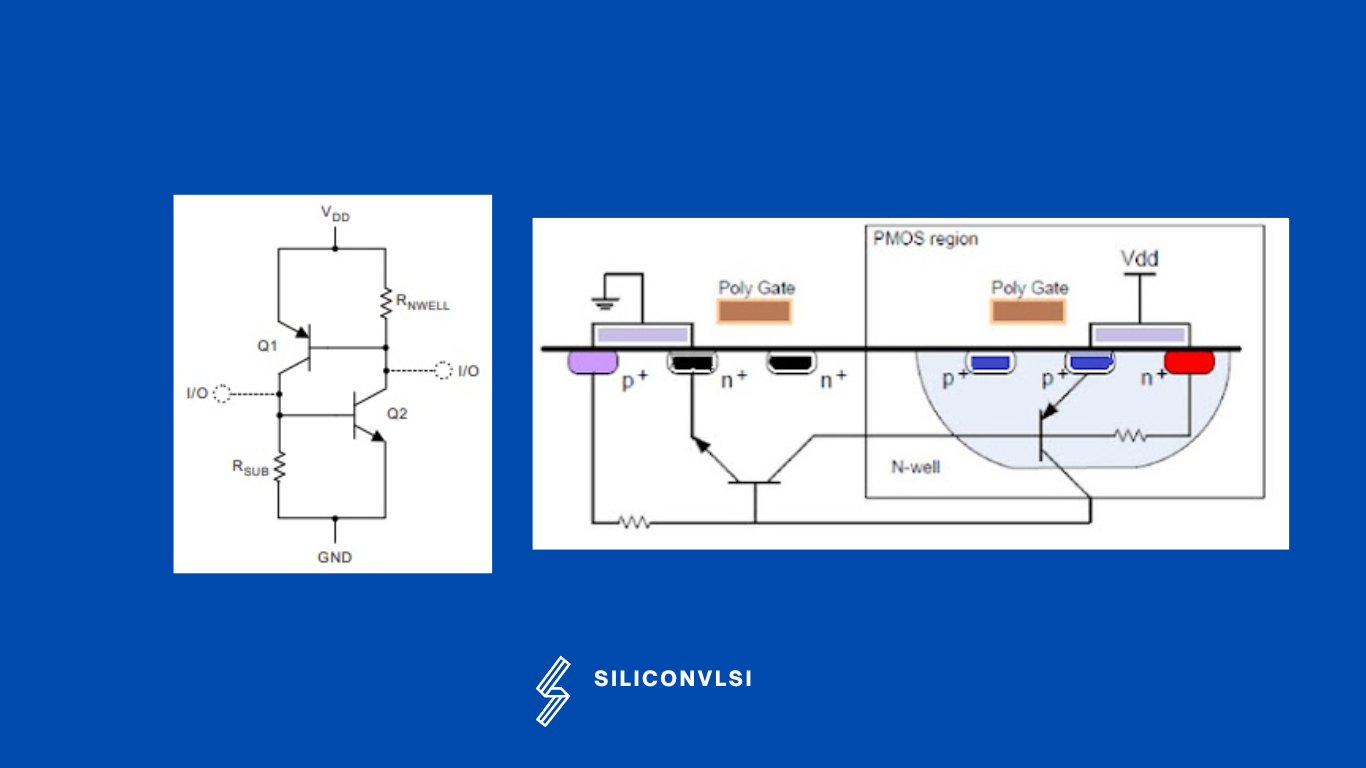
Latchup is a phenomenon in integrated circuits (ICs) where a short circuit or low-impedance path is created between the power and ground rails, resulting in high current flow and potential damage to the IC. This occurs due to the interaction between parasitic pnp (positive-negative-positive) and npn (negative-positive-negative) transistors within the IC. The structure formed by these transistors resembles that of a Silicon Controlled Rectifier (SCR), allowing for unintended current flow and causing latch-up.
Reason for the Latch-up
- Low Impedance path between Substrate and well.
- Minority carriers inject into the substrate or well
- Short circuit between Vdd and Vss
- Temperature effects can also influence the Latch-Up immunity of products. because as temperature increases, the substrate and well resistances rise to allow the bias to reach a critical value sooner.
- The effective distance between the N+, P+, and N-Well diffusion narrows allowing easier capture of excited carriers.
How to reduce the latch-up effect || How to avoid the Latch-up effect.
- Use More Tap(Bulk) for Digital Circuit Layout
- Use a Guard ring for the Analog layout.
- Keep more distance between Pmos & Nmos
- Give more Enclosure of Newell
- Use the halo doping concept
- Use an EPI(epitaxial layer) layer.