Close Menu
  • Analog Design
    • Latest Analog Layout Interview Questions (2025)
  • Digital Design
    • Digital Electronics Interview Question(2025)
    • Top VLSI Interview Questions
  • Physical Design
    • Physical Design Interview Questions for VLSI Engineers
  • Verilog
    • Verilog Interview Questions(2024)
  • Forum
Facebook Instagram YouTube LinkedIn WhatsApp
SiliconvlsiSiliconvlsi
Forum Questions Register in Forum Login in Forum
Facebook Instagram YouTube LinkedIn WhatsApp
  • Analog Design
    • Latest Analog Layout Interview Questions (2025)
  • Digital Design
    • Digital Electronics Interview Question(2025)
    • Top VLSI Interview Questions
  • Physical Design
    • Physical Design Interview Questions for VLSI Engineers
  • Verilog
    • Verilog Interview Questions(2024)
  • Forum
SiliconvlsiSiliconvlsi
Home»VLSI Design»Contact Cut
VLSI Design

Contact Cut

siliconvlsiBy siliconvlsiOctober 3, 2023Updated:May 21, 2024No Comments1 Min Read
Facebook Pinterest LinkedIn Email WhatsApp
Share
Facebook Twitter LinkedIn Pinterest Email

What is Contact Cut?

A contact cut refers to an opening or hole in a layer of material, typically an insulator-like oxide, that allows for an electrical contact or connection between different layers in a semiconductor device. In the provided paragraph:

Contact Cut
Contact Cut
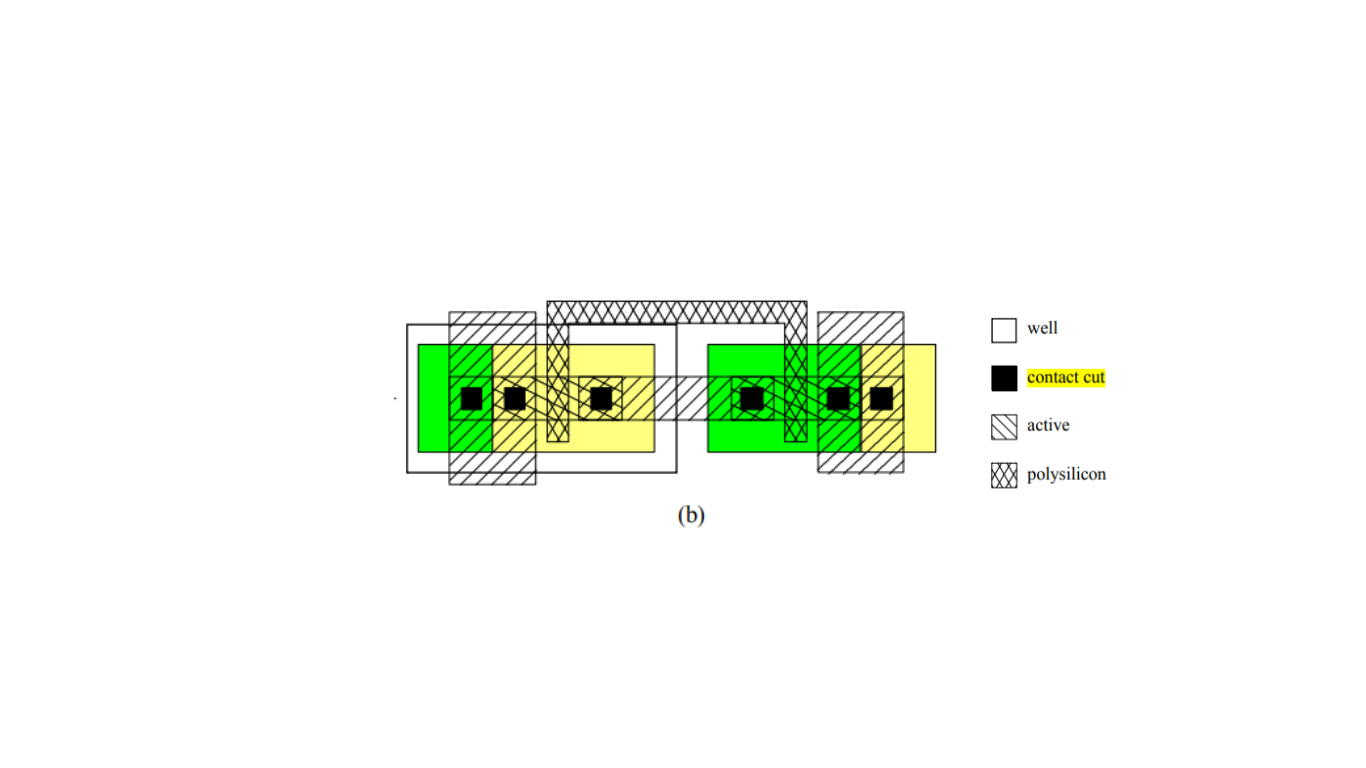
  • Definition with a Mask The contact cuts are created using a masking process. A mask is used to define the specific locations where these contact cuts need to be made on the wafer.
  • Material Filling  After defining the contact cuts, they are often filled with a material to ensure electrical connectivity. In this case, tungsten is mentioned as a common material used for this purpose.

These contact cuts play a crucial role in creating paths for interconnecting different layers of the semiconductor device. Once the contact cuts are defined and filled, subsequent layers, such as a thin layer of aluminum, can be deposited and patterned to form the interconnections that link various components of the semiconductor device. The contact cuts enable electrical communication between different levels or layers in the integrated circuit.

Share. Facebook Twitter Pinterest LinkedIn Tumblr Email

Related Posts

How Shielding Avoids Crosstalk Problem? What Exactly Happens There?

September 22, 2024

Navigating the Challenges of Gate Dielectric Scaling in MOS Transistors

August 1, 2024

Challenges in Modern SoC Design Verification

April 20, 2024
Leave A Reply Cancel Reply

Facebook X (Twitter) Instagram Pinterest Vimeo YouTube
  • About Us
  • Contact Us
  • Privacy Policy
© 2025 Siliconvlsi.

Type above and press Enter to search. Press Esc to cancel.