
What is a Deep sub-micron?
“Deep sub-micron” refers to technology nodes or processes with feature sizes that are smaller than one micrometer (micron). Typically, it refers to dimensions at or below 0.25 micrometers. The term “sub-micron” originally referred to feature sizes smaller than one micron, but as technology advanced, “deep sub-micron” emerged to specifically denote even smaller feature sizes.
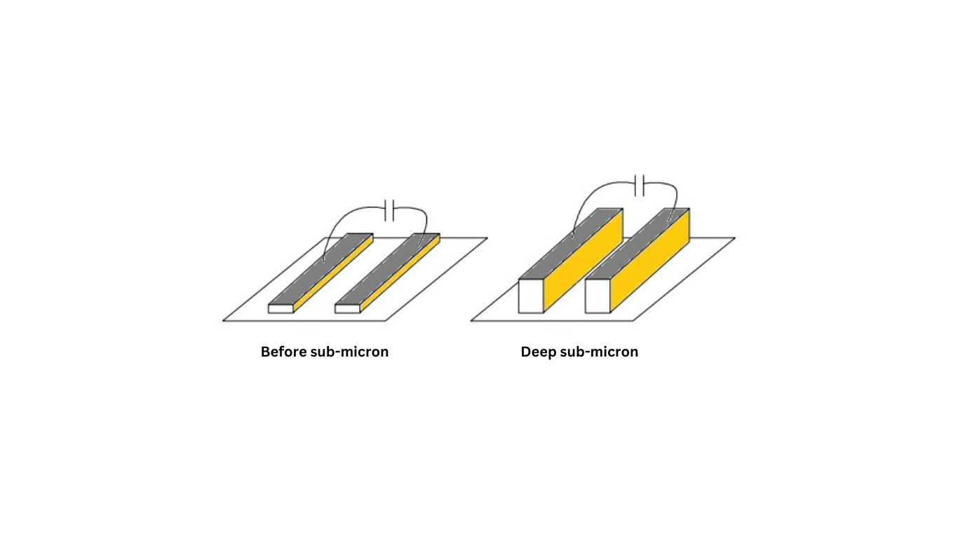
In deep sub-micron designs (0.25 micrometers or below), the thickness or height of wires becomes relatively more significant, and the capacitance between parallel wires becomes a significant factor. This presents challenges in accurately extracting parasitic capacitance and resistance, making it a major research area in semiconductor design.
What are some of the key features introduced in deep submicron CMOS technologies?
Deep submicron CMOS technologies introduce several new features and techniques that significantly influence device characteristics and circuit design:
Shallow Trench Isolation (STI): STI replaces Local Oxidation and alters device profiles and leakage current characteristics. Measurements have shown that STI does not degrade compared to LOCOS, and some devices maintain consistent leakage current levels even under radiation exposure.
Dual Gate Implants: This standard feature allows individual threshold adjustment for both N and P devices, enhancing control over device performance.
Thin Gate Oxides: Standard gate oxides of approximately 45-60 Angstroms are fundamental to achieving total-dose radiation hardness in 0.25-micron technologies.
Shallow Lightly Doped Drain (LDD) Structures: LDD structures are essential for minimizing short-channel effects in transistors.
Silicided Source and Drain: These structures are crucial for reducing series resistance to metal contacts and providing an extra free metal level. However, they may not always be suitable for analog applications.
Lower Supply Voltage (VDD): A standard VDD of 2.5 volts is common in 0.25-micron gate length technologies, impacting circuit configurations. Manufacturers offer options for NMOS devices with threshold voltages close to 0 volts, catering to analog circuit needs.
Increasing Number of Metal Interconnect Levels: Commercial microprocessors now incorporate up to 5 or more metal interconnect levels, a crucial factor for most circuits. However, its impact on HEP (High Energy Physics) designs, particularly mixed-signal circuits, is relatively small.
Advanced Bonding Techniques: Manufacturers are introducing advanced bonding methods like bump-bonding or tape techniques, which can profoundly affect HEP ASICs. These technologies can reduce costs and improve reliability but necessitate testability features based on scan-path in circuit design.
BiCMOS Option: Some foundries offer BiCMOS options, including SiGe bipolar devices with high fT values (> 50 GHz), primarily targeted at high-speed RF and telecom components.
These features and developments in deep submicron CMOS technologies have a significant impact on semiconductor devices and circuit design, influencing factors such as performance, power consumption, and radiation tolerance.