
When designing CMOS devices, it is important to take into account the effects of DIBL, GIDL, BTBT, and Tunneling. These phenomena can significantly impact the functionality of the design. Understanding these terms is of utmost importance in VLSI design. In this article, we will delve into each effect and explore its implications.
Drain Induced Barrier Lowering (DIBL)
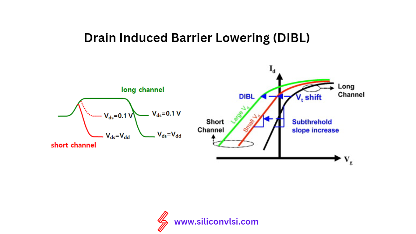
DIBL, or Drain-Induced Barrier Lowering, in MOSFETs, causes a reduction in the threshold voltage (Vth) of transistors at high drain-to-source voltage (Vds). As Vds increases, Vth decreases according to the following equation:
Vth = Vt0 – n * Vds
Additionally, DIBL increases the subthreshold leakage at higher drain voltage (Vds).
Gate Induced Drain Leakage (GIDL)
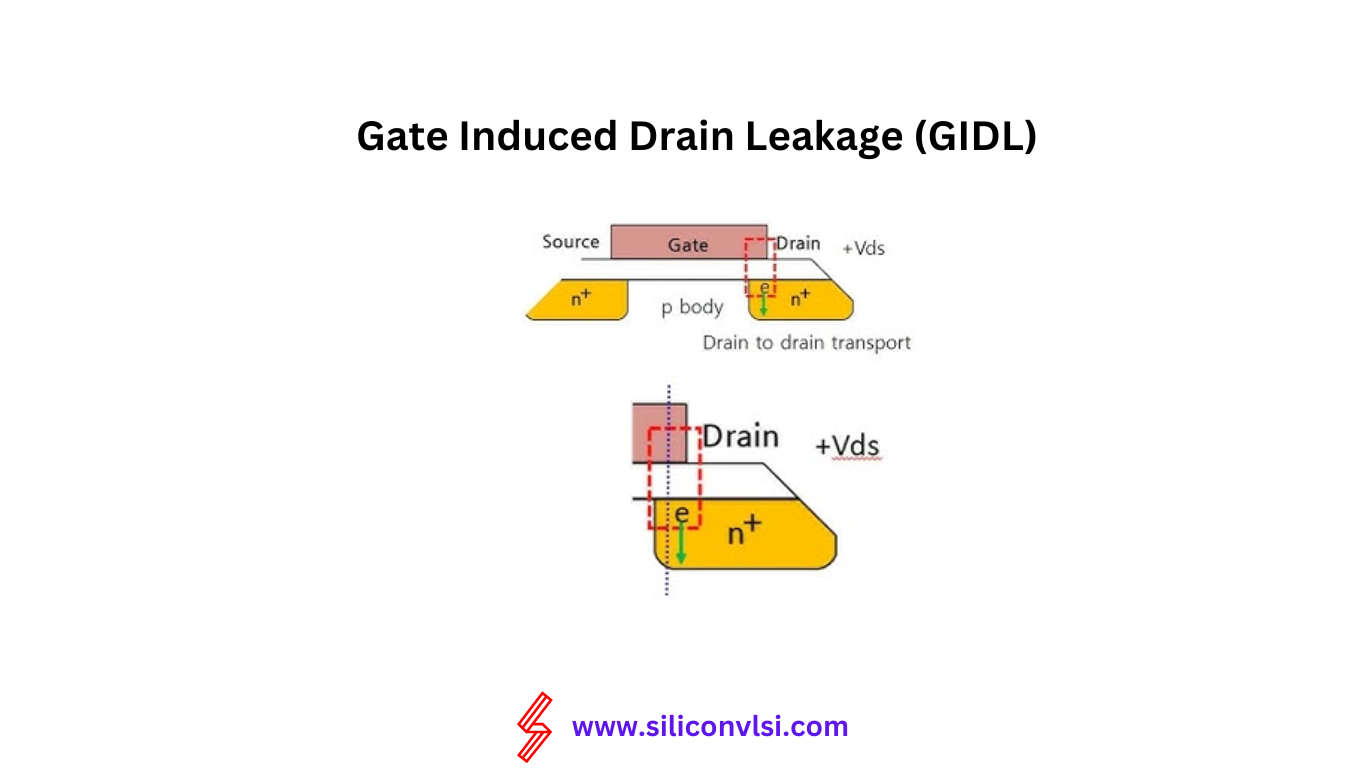
GIDL, or Gate Induced Drain Leakage, occurs when the gate partially overlaps with the drain of the MOSFET. It becomes more pronounced when VDD or Vds levels are at high potential, while Vgs are at a low potential. The magnitude of GIDL is directly proportional to the gate-drain overlap area, and transistor width is insignificant when Vgd <= VDD (gate-to-drain voltage is less than or equal to the supply voltage).
When Vgs < 0, it causes the depletion region between the PN-junction to thin out. As the substrate is at a low potential, the minority charge carriers formed underneath the gate scatter laterally.
Band to Band Tunneling (BTBT)
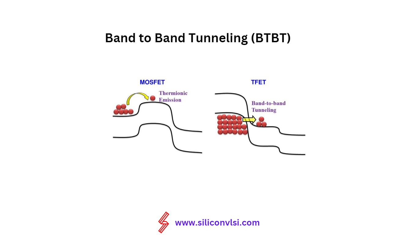
BTBT, or Band to Band Tunneling, occurs across the junction between the source and the body, or drain and the body of the transistor when the junction is reverse biased. It describes the carrier generation in the high-field region without any influence of local traps.
BTBT is influenced by reverse bias and doping levels. Typically, high halo doping is utilized to increase the threshold voltage (Vth) and reduce subthreshold leakage. However, it inadvertently causes BTBT to grow. The leakage caused by Trap Assisted Tunneling (TAT) arises when defects in the Silicon Lattice, known as traps, reduce the distance that a carrier must travel.
Tunneling Effect
The tunneling effect can be categorized into two types:
- FN tunneling effect
- Direct tunneling effect
The figure above illustrates the electron flow due to the tunneling effect from the substrate to the gate. This process involves carrier tunneling through the gate oxide (SiO2), resulting in a gate leakage current. As the gate voltage increases, the tunneling current also increases, as shown in the graph above. The likelihood of this tunneling effect reduces exponentially with the oxide thickness (tox). In certain cases, the tunneling effect can be intentionally utilized to create electrically erasable memory devices, such as EEPROM.