Close Menu
  • Analog Design
    • Latest Analog Layout Interview Questions (2025)
  • Digital Design
    • Digital Electronics Interview Question(2025)
    • Top VLSI Interview Questions
  • Physical Design
    • Physical Design Interview Questions for VLSI Engineers
  • Verilog
    • Verilog Interview Questions(2024)
  • Forum
Facebook Instagram YouTube LinkedIn WhatsApp
SiliconvlsiSiliconvlsi
Forum Questions Register in Forum Login in Forum
Facebook Instagram YouTube LinkedIn WhatsApp
  • Analog Design
    • Latest Analog Layout Interview Questions (2025)
  • Digital Design
    • Digital Electronics Interview Question(2025)
    • Top VLSI Interview Questions
  • Physical Design
    • Physical Design Interview Questions for VLSI Engineers
  • Verilog
    • Verilog Interview Questions(2024)
  • Forum
SiliconvlsiSiliconvlsi
Home»VLSI Design»Difference between Layout and Schematic
VLSI Design

Difference between Layout and Schematic

siliconvlsiBy siliconvlsiAugust 21, 2022Updated:May 12, 2024No Comments2 Mins Read
Facebook Pinterest LinkedIn Email WhatsApp
Share
Facebook Twitter LinkedIn Pinterest Email

Difference between Layout and Schematic

The difference between Layout and Schematic is Layout is a Physical representation of a Schematic and Schematic is a topological representation of the circuit.

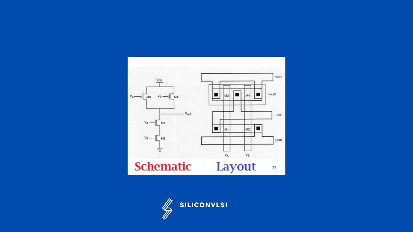
A geometric model of the circuit is called layout (circuit board layout). It is mainly meant for fabrication. If necessary, various layouts for the same schematic can be created. Schematics are simpler to read and comprehend when compared to layout, yet they may not always provide a complete picture of the circuit’s physical implementation.

The schematic is a drawing that shows the logical connections between the components. In essence, it demonstrates how the parts are electrically connected. A netlist, a straightforward data structure seen in a schematic, is used to list each connection in the design according to the drawing’s specifications. A schematic diagram is given in the figure below.

Difference between Layout and Schematic

Rules to draw  a schematic 

  • Put the outputs on the right and the inputs to the left.
  • Design functional blocks in the schematic parts.
  • Pin numbers should always be placed outside any symbol graphics.
  • It is best to write the pin numbers, polarity, values, and net names horizontally.
  • Symbols for sheet connections should always be positioned on the page’s extreme left- or right-hand edges.

Rules to Draw a Layout

  • Give Nwell to Nwell more space
  • Avoid jogs in metal
  • Try to maintain the same environment in Layout
  • Put more number of vias
  • Use proper power mesh
  • Share the same diffusion


Share. Facebook Twitter Pinterest LinkedIn Tumblr Email

Related Posts

How Shielding Avoids Crosstalk Problem? What Exactly Happens There?

September 22, 2024

Navigating the Challenges of Gate Dielectric Scaling in MOS Transistors

August 1, 2024

Challenges in Modern SoC Design Verification

April 20, 2024
Leave A Reply Cancel Reply

Facebook X (Twitter) Instagram Pinterest Vimeo YouTube
  • About Us
  • Contact Us
  • Privacy Policy
© 2025 Siliconvlsi.

Type above and press Enter to search. Press Esc to cancel.