

Difference between Schematic and Layout.
A Schematic is a “Circuit Diagram” or a drawing of how it will work. A “Layout” is the circuit board or Physical representation of the schematic.
What is Schematic Diagram?
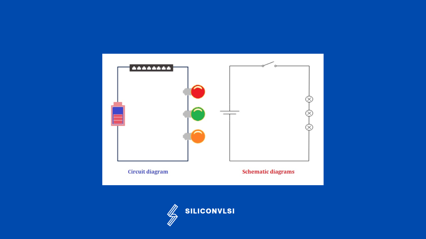
The schematic is a drawing that defines the logical connections between components on a circuit board whether it is a rigid PCB or a flex board. A schematic diagram is a visual representation of a process, device, or other object’s parts using standardized, frequently abstract symbols and lines. Although schematic diagrams are frequently related to electrical circuits, there are numerous instances in other fields as well.
Rules for drawing schematic diagram
- Wires must not cross and connect.
- Label pin numbers on the outside of a symbol, and signal names on the inside.
- Any critical or Matching device information should be mentioned in text format.
- Wires and components are aligned horizontally or vertically unless there’s a good reason to do otherwise.
Differences between Schematic Diagrams and Circuit Diagrams
Engineering diagrams frequently make use of schematics and circuit diagrams. Even though you’ve probably heard them a lot, they do differ differently from one another. Their intended audiences or readers are different; whereas skilled schematic viewers frequently use schematics, beginners can easily understand circuit diagrams.
You will have a thorough understanding of the usefulness of diagrams in identifying the parts of an electric system, tracing a circuit, or even fixing electrical equipment after seeing an illustration of the distinctions between schematic diagrams and circuit diagrams.
What is Layout?
A larger integrated circuit is created using a VLSI layout, which incorporates many smaller circuits. Building essential circuit blocks and incorporating them into a bigger system are the first steps in this design technique. A series of circuit simulations are utilized to optimize each circuit block when creating circuit blocks prior to the VLSI layout.
Layout design rules VLSI
On MOSIS rules, design regulations are based. Parameter lambda is the most important phrase in MOSIS rules. There are several levels of design rules.
- Well, rules
- Transistor rules
- Contact rules
- Metal rules
- Via rules
Well Rules
- N-well transistor implants are put more deeply than any other type. The distance between the margins of n-wells and the diffusion of n+ should be sufficient. Typically, the oxide transition time across the good barrier determines this clearance. The second guideline calls for grounding n-well and ensuring an adequate number of good taps. Due to the well current, this will stop severe voltage dips.
Transistor rules
- Polysilicon mask – crossing of polysilicon and diffusion mask defines the gates of the transistor.
- Active mask – defines where p- or n-diffusion type or gates will be placed.
- n-implant mask – defines areas where n-type diffusion is required.
- p-implant mask – defines where p-type diffusion is required.
Contacts rules
- metal to p-active
- metal to n-active
- metal to polysilicon
- metal to well or substrate
Metal rules
- Depending on the metal line, the metal spacing rule may vary. However, both thin and thick wires must adhere to a particular width. Therefore, if wider cables are required, they can be created by connecting numerous small wires. Long parallel wires can be arranged according to spacing regulations.
Why Are Schematic and Layout Both Important?
A circuit can have a correct schematic but still have an incorrect layout.
For example, the layout may contain:
- Incorrect connectivity
- Missing contacts
- Insufficient spacing
- Incorrect device dimensions
- Poor matching
- Excessive parasitic capacitance
- Excessive resistance
- Substrate noise coupling
Therefore, schematic verification alone is not sufficient.
Similarly, a layout can satisfy geometric rules but still not represent the intended circuit. This is why LVS is important.
Schematic vs Layout: A Simple Example
Consider a CMOS inverter.
Schematic
The schematic shows:
PMOS → VDD
NMOS → GND
PMOS + NMOS gates → Input
PMOS + NMOS drains → Output
This tells us the electrical connectivity.
Layout
The layout physically creates:
- PMOS active region
- NMOS active region
- Polysilicon gate
- Well region
- Contacts
- Metal connections
The physical arrangement determines the actual geometry and therefore influences parasitic resistance and capacitance.
Common Mistakes in Schematic and Layout
Mistake 1: Assuming a Correct Schematic Guarantees Correct Layout
It does not.
The layout must be independently verified.
Mistake 2: Ignoring Parasitics
Long metal routes and large device structures can introduce significant parasitic capacitance and resistance.
Mistake 3: Treating DRC as an LVS Check
DRC checks geometric/manufacturing rules.
LVS checks electrical correspondence between layout and schematic.
They are different verification steps.
Mistake 4: Ignoring Matching Requirements
For analog circuits, simply placing matching devices close together may not be sufficient.
Techniques such as:
- Common-centroid layout
- Interdigitation
- Dummy devices
- Symmetry
- Identical orientation
may be required depending on the circuit.
Mistake 5: Using Universal Layout Rules
There is no single set of physical dimensions that applies to every CMOS technology.
Always use the rules provided by the relevant foundry PDK.
Frequently Asked Questions
What is the main difference between schematic and layout?
A schematic represents the electrical connectivity and circuit structure, while a layout represents the physical implementation of that circuit on silicon.
Is layout the physical representation of a schematic?
Yes. In VLSI, layout is the physical implementation of the circuit described by the schematic.
What is checked in DRC?
DRC checks whether the physical layout satisfies the manufacturing and geometric rules of the target technology.
What is checked in LVS?
LVS compares the connectivity and device information extracted from the layout against the intended schematic.
Can a layout pass DRC but fail LVS?
Yes. A layout can satisfy all geometric design rules while still having incorrect electrical connectivity or incorrect device structure.
Why is post-layout simulation required?
Layout introduces parasitic resistance and capacitance that are not fully represented in an ideal schematic. Post-layout simulation evaluates circuit behavior with those extracted effects included.
Conclusion
The difference between a schematic and layout can be summarized in one sentence:
A schematic describes what the circuit is; a layout describes how that circuit is physically built.
The schematic is primarily concerned with electrical connectivity and circuit behavior, while the layout is concerned with physical geometry, manufacturing constraints, parasitics, and physical implementation.
A successful VLSI design requires both to agree. That is why DRC, LVS, parasitic extraction, and post-layout simulation are essential parts of the physical design flow.