
Close Menu
  • Analog Design
    • Latest Analog Layout Interview Questions
  • Digital Design
    • Digital Electronics Interview Question
    • Top VLSI Interview Questions
  • Physical Design
    • Physical Design Interview Questions for VLSI Engineers
  • Verilog
    • Verilog Interview Questions(2026)
  • Forum
  • Calculators
    • Asynchronous FIFO Depth Calculator
    • Clock Skew and Clock Jitter Calculator
    • Setup Time Calculator
Facebook Instagram YouTube LinkedIn WhatsApp
SiliconvlsiSiliconvlsi
Ask Questions Register in Forum Login in Forum
Facebook Instagram YouTube LinkedIn WhatsApp
  • Analog Design
    • Latest Analog Layout Interview Questions
  • Digital Design
    • Digital Electronics Interview Question
    • Top VLSI Interview Questions
  • Physical Design
    • Physical Design Interview Questions for VLSI Engineers
  • Verilog
    • Verilog Interview Questions(2026)
  • Forum
  • Calculators
    • Asynchronous FIFO Depth Calculator
    • Clock Skew and Clock Jitter Calculator
    • Setup Time Calculator
SiliconvlsiSiliconvlsi
Home ยป Wells, Taps, and Guard rings
Analog Design

Wells, Taps, and Guard rings

siliconvlsiBy siliconvlsiJanuary 4, 2022Updated:August 24, 2026No Comments1 Min Read
Facebook Pinterest LinkedIn Email WhatsApp
Share
Facebook Twitter LinkedIn Pinterest Email

Wells, Taps, and Guard ring.

Most CMOS processes are constructed with a P-type bulk substrate and NMOS devices are constructed by implanting N-type source and drain geometry.

To construct a PMOS device a region of N-type material is needed. The N-type material is called the N-well and it surrounds the P-type source and drains geometry to create the MOSFET channel.
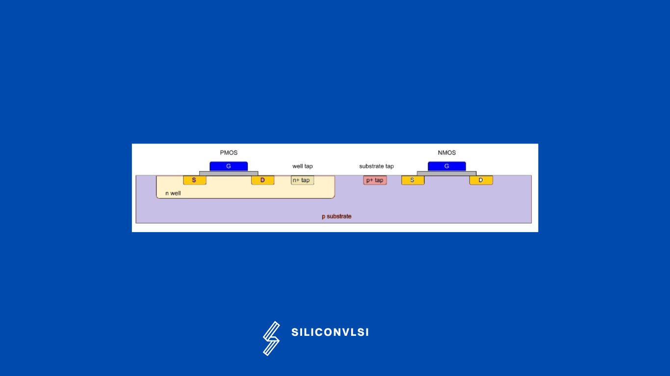
Well has a good electrical connection to power the N-well and ground for the P-well. This connection is achieved by inserting taps and/or guard rings into the layout.

A guard is essentially a ring-shaped tap that wraps around the transistors. Taps and guard rings also reduce the likelihood of latch-up, where a low impedance path between the power rails is formed, creating a damagingly high current through the circuit

Share. Facebook Twitter Pinterest LinkedIn Tumblr Email

Related Posts

BJTs vs. MOSFETs: Key Differences Every Analog Designer Should Know

April 3, 2025

What is 2.5D Approach in Packaging Technology

December 1, 2024

Analog Layout Interview Questions with Answer 2026

August 3, 2024
Leave A Reply Cancel Reply

Facebook X (Twitter) Instagram Pinterest Vimeo YouTube
  • About Us
  • Contact Us
  • Privacy Policy
© 2026 Siliconvlsi.

Type above and press Enter to search. Press Esc to cancel.