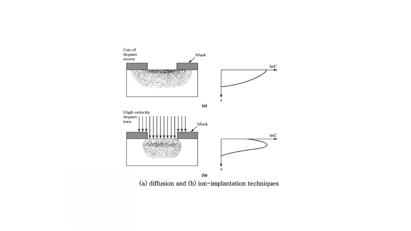
Integrated circuit manufacturing often requires altering the dopant concentration in specific regions of semiconductor materials. This alteration is essential for creating various components like source and drain regions, adjusting device thresholds, and forming well and substrate contacts. Two primary methods for introducing dopants into semiconductor materials are diffusion and ion implantation, each with its distinct processes and impacts.

Diffusion
In the diffusion process, semiconductor wafers are placed in a heated furnace typically ranging from 900 to 1100°C. A gas containing the desired dopant is introduced into the furnace tube. The high temperatures cause the dopant atoms to diffuse into the exposed surface of the semiconductor material, spreading both vertically and horizontally. As a result, the final dopant concentration is highest at the surface and gradually decreases deeper into the material. The diffusion process follows a Gaussian profile.
Ion Implantation
Ion implantation involves introducing dopants as ions into the semiconductor material. An ion implantation system directs a beam of purified ions over the surface of the semiconductor. The depth to which the ions penetrate is determined by their acceleration, while the dosage (concentration) is controlled by adjusting the beam current and exposure time. This technique provides independent control over the depth and dosage of dopants, making it highly precise.
Differences and Impacts
Control: Ion implantation offers superior control over dopant depth and dosage compared to diffusion, making it the preferred choice in modern semiconductor manufacturing.
Lattice Damage: Ion implantation can cause lattice damage due to nuclear collisions during high-energy implantation, leading to material defects. This issue is typically resolved through a subsequent annealing process, which involves heating the wafer to around 1000°C for a specific duration and then slowly cooling it. Annealing helps atoms re-form bonds and mitigates lattice damage.
In summary, both diffusion and ion implantation are techniques for introducing dopants into semiconductor materials during integrated circuit manufacturing. While diffusion relies on temperature-induced diffusion of dopants, ion implantation offers precise control over depth and dosage. However, ion implantation can lead to lattice damage, which is addressed through annealing. The choice between these techniques depends on the specific requirements of the semiconductor manufacturing process.
What are the two main methods used for introducing dopants into semiconductor materials during integrated circuit manufacturing?
The two main methods for introducing dopants into semiconductor materials during integrated circuit manufacturing are diffusion and ion implantation.
How does diffusion implantation work, and what conditions are typically required for this process?
In diffusion implantation, wafers are placed in a heated furnace within a quartz tube. A gas containing the dopant is introduced into the tube. The high temperatures, typically between 900 to 1100 °C, cause the dopants to diffuse into the exposed surface of the semiconductor material, both vertically and horizontally. The dopant concentration is highest at the surface and decreases deeper into the material in a Gaussian profile.
What is ion implantation, and how does it differ from diffusion implantation in terms of dopant introduction?
Ion implantation involves introducing dopants as ions into the semiconductor material. An ion implantation system directs and sweeps a beam of purified ions over the semiconductor surface. The depth of ion penetration is determined by the ion’s acceleration, while the dosage is controlled by the beam current and exposure time. Ion implantation provides independent control over both the depth and dosage of dopants, making it a preferred method in modern semiconductor manufacturing.
What is a significant drawback of ion implantation, and how is it typically addressed?
A major drawback of ion implantation is lattice damage caused by nuclear collisions during high-energy implantation. This can lead to material defects. To address this issue, a subsequent annealing step is applied, where the wafer is heated to around 1000°C for 15 to 30 minutes and then allowed to cool slowly. This heating process thermally vibrates the atoms, allowing bonds to reform and mitigating the lattice damage.
Why has ion implantation largely replaced diffusion in modern semiconductor manufacturing?
Answer: Ion implantation has largely replaced diffusion in modern semiconductor manufacturing because it offers precise control over both the depth and dosage of dopants. This level of control is crucial for achieving the desired electrical properties in semiconductor devices.