Close Menu
  • Analog Design
    • Latest Analog Layout Interview Questions (2025)
  • Digital Design
    • Digital Electronics Interview Question(2025)
    • Top VLSI Interview Questions
  • Physical Design
    • Physical Design Interview Questions for VLSI Engineers
  • Verilog
    • Verilog Interview Questions(2024)
  • Forum
Facebook Instagram YouTube LinkedIn WhatsApp
SiliconvlsiSiliconvlsi
Ask Questions Register in Forum Login in Forum
Facebook Instagram YouTube LinkedIn WhatsApp
  • Analog Design
    • Latest Analog Layout Interview Questions (2025)
  • Digital Design
    • Digital Electronics Interview Question(2025)
    • Top VLSI Interview Questions
  • Physical Design
    • Physical Design Interview Questions for VLSI Engineers
  • Verilog
    • Verilog Interview Questions(2024)
  • Forum
SiliconvlsiSiliconvlsi
Home»VLSI Design»Optimizing Noise Margins in VLSI System Design | VLSI Design
VLSI Design

Optimizing Noise Margins in VLSI System Design | VLSI Design

siliconvlsiBy siliconvlsiMay 23, 2023Updated:December 20, 2024No Comments2 Mins Read
Facebook Pinterest LinkedIn Email WhatsApp
Share
Facebook Twitter LinkedIn Pinterest Email

What Is Noise Margin in VLSI

What Is Noise Margin in VLSI Design

Noise margins represent the difference between the minimum voltage level that represents a logic high (logic ‘1’) and the maximum voltage level that represents a logic low (logic ‘0’). They define the voltage range within which we can correctly interpret and distinguish logic levels. In other words, noise margins provide a buffer zone to account for variations in signal levels caused by noise.

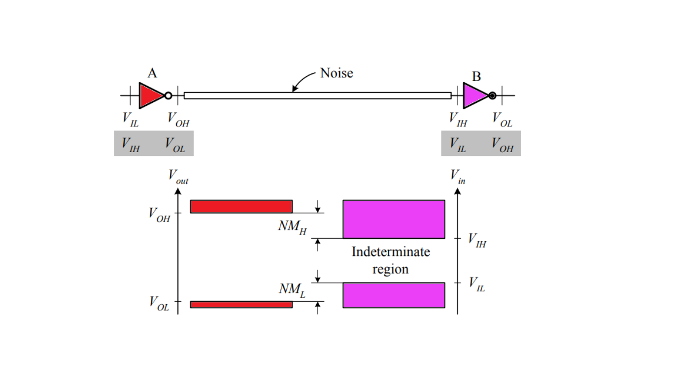
Types of Noise Margins

There are two main types of noise margins in VLSI design: the noise margin for a logic high (NMH) and the noise margin for a logic low (NML). NMH is the difference between the minimum voltage level for a logic high and the maximum voltage level for a logic low. That is, both NMH and NML can be expressed as follows.

NMH = VOH − VIH
NML = VIL − VOL

Four voltage levels are established to indicate input and output voltage values, allowing two logic circuits of the same or different families to be cascaded while tolerating process, voltage, and temperature (PVT) fluctuations. The input logic 0 and 1, respectively, are specified by the two input voltage levels VIL and VIH. The output logic 0 and 1.1 are specified individually using the two output voltage levels VOL and VOH. These four voltage levels are specified more specifically as follows.

VIH (high-level input voltage) is the minimum high input voltage to be recognized as logic 1.

VIL (low-level input voltage) is the maximum low input voltage to be recognized as logic 0.

VOH (high-level output voltage) is the minimum high output voltage when the output is logic 1.

VOL (low-level output voltage) is the maximum low output voltage when the output is logic 0.

Share. Facebook Twitter Pinterest LinkedIn Tumblr Email

Related Posts

How Shielding Avoids Crosstalk Problem? What Exactly Happens There?

September 22, 2024

Navigating the Challenges of Gate Dielectric Scaling in MOS Transistors

August 1, 2024

Challenges in Modern SoC Design Verification

April 20, 2024
Leave A Reply Cancel Reply

Facebook X (Twitter) Instagram Pinterest Vimeo YouTube
  • About Us
  • Contact Us
  • Privacy Policy
© 2025 Siliconvlsi.

Type above and press Enter to search. Press Esc to cancel.