Close Menu
  • Analog Design
    • Latest Analog Layout Interview Questions (2025)
  • Digital Design
    • Digital Electronics Interview Question(2025)
    • Top VLSI Interview Questions
  • Physical Design
    • Physical Design Interview Questions for VLSI Engineers
  • Verilog
    • Verilog Interview Questions(2024)
  • Forum
Facebook Instagram YouTube LinkedIn WhatsApp
SiliconvlsiSiliconvlsi
Forum Questions Register in Forum Login in Forum
Facebook Instagram YouTube LinkedIn WhatsApp
  • Analog Design
    • Latest Analog Layout Interview Questions (2025)
  • Digital Design
    • Digital Electronics Interview Question(2025)
    • Top VLSI Interview Questions
  • Physical Design
    • Physical Design Interview Questions for VLSI Engineers
  • Verilog
    • Verilog Interview Questions(2024)
  • Forum
SiliconvlsiSiliconvlsi
Home»VLSI Design»Doping in Physics
VLSI Design

Doping in Physics

siliconvlsiBy siliconvlsiJuly 11, 2023Updated:May 17, 2024No Comments1 Min Read
Facebook Pinterest LinkedIn Email WhatsApp
Share
Facebook Twitter LinkedIn Pinterest Email

To boost a semiconductor’s conductivity, impurity atoms are added to a pure or intrinsic semiconductor through the process called “doping.” There are two methods of doping: adding an n-type dopant or adding a pentavalent dopant to an intrinsic semiconductor to create an n-type semiconductor.

Doping: n- and p-semiconductors

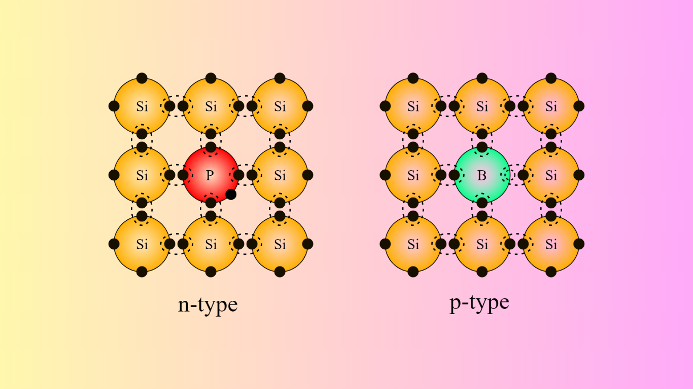
An n-type semiconductor is created when group V elements like phosphorus and arsenic are doped in group IV elements (Si or Ge). The extra negative charges caused by the impurity’s extra electrons are what cause the electrical conduction.
A p-type semiconductor is created when group III elements like boron and gallium are doped with group IV elements (Si or Ge). The extra positive charges caused by the impurity’s electron holes are what cause the electrical conduction.


Conditions Required for the Doping Process

The atom that needs to be doped in the crystal must be positioned exactly where the semiconductor atom is.

After the dopants have been inserted, the crystal shouldn’t have any distortion.

The size of the dopants should exactly match the size of the crystal’s atoms.

The amount of doping in a crystal shouldn’t be greater than 1%.

Share. Facebook Twitter Pinterest LinkedIn Tumblr Email

Related Posts

How Shielding Avoids Crosstalk Problem? What Exactly Happens There?

September 22, 2024

Navigating the Challenges of Gate Dielectric Scaling in MOS Transistors

August 1, 2024

Challenges in Modern SoC Design Verification

April 20, 2024
Leave A Reply Cancel Reply

Facebook X (Twitter) Instagram Pinterest Vimeo YouTube
  • About Us
  • Contact Us
  • Privacy Policy
© 2025 Siliconvlsi.

Type above and press Enter to search. Press Esc to cancel.