Doping in VLSI
Doping is the introduction of controlled amounts of impurities into semiconductors to change their electrical properties. Diffusion and ion implantation are the main methods for impurity doping. The fabrication of discrete devices and integrated circuits uses both diffusion and ion implantation because these procedures frequently work well together. For instance, ion implantation is used to generate a shallow junction(e.g., a source-drain junction of a MOSFET), whereas diffusion is used to form deep junctions (such as a twin well in CMOS) .
What is the function of doping?
The primary objective of doping is to alter the electrical properties of the semiconductor by introducing impurities, thereby modifying the concentration of charge carriers such as electrons (for n-type doping) or holes (for p-type doping). This alteration in concentration affects the material’s conductivity and, consequently, its electrical characteristics.
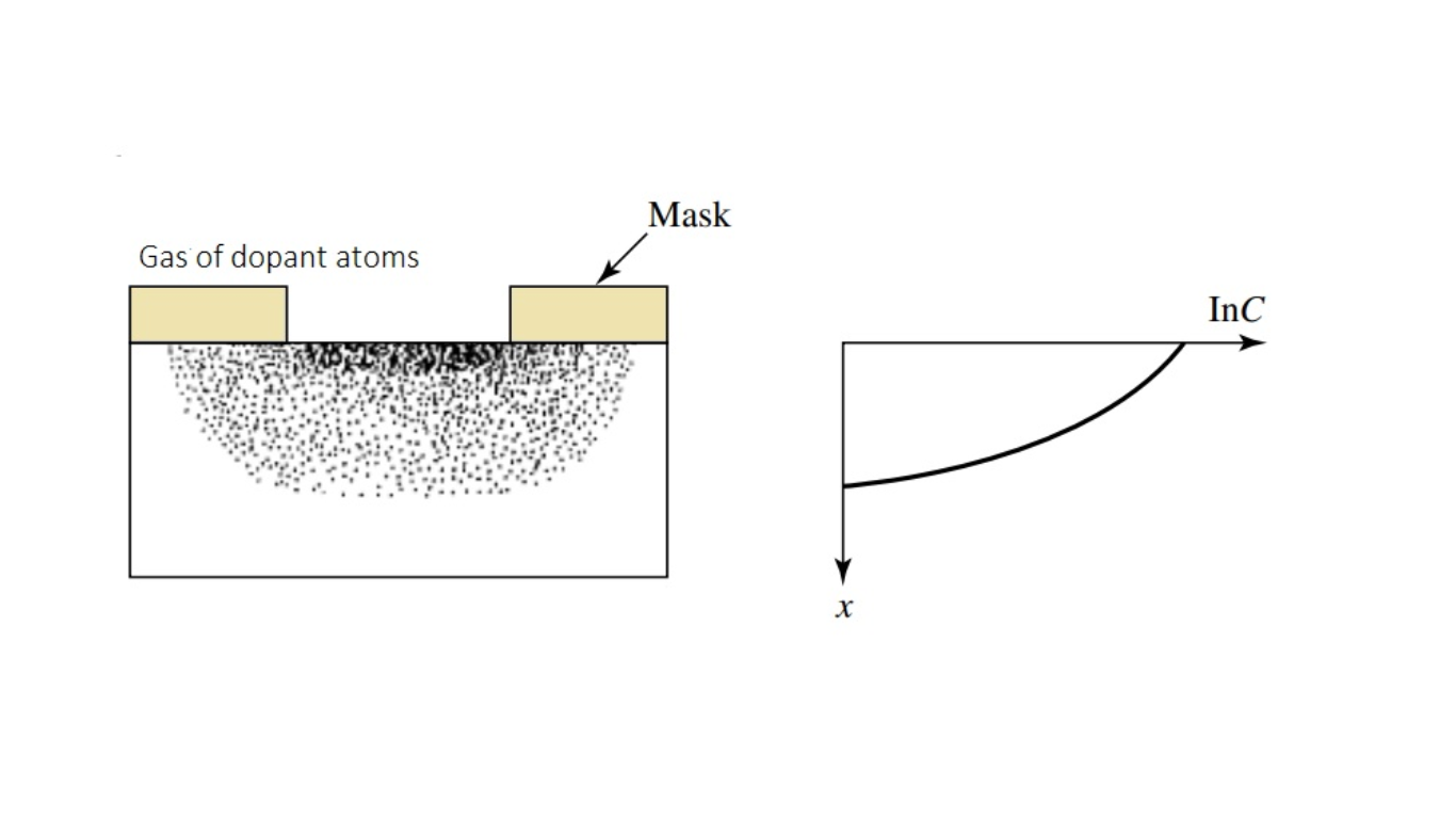
Diffusion
In the early 1970s, impurity doping was performed by diffusion at some temperatures, as shown in Figure 1. In this method, the dopant atoms are placed on or near the surface of the wafer by deposition from the gas phase of the dopant or by using doped-oxide sources. The doping concentration decreases monotonically from the surface, and the profile of the dopant distribution is determined mainly by the temperature and the diffusion time.
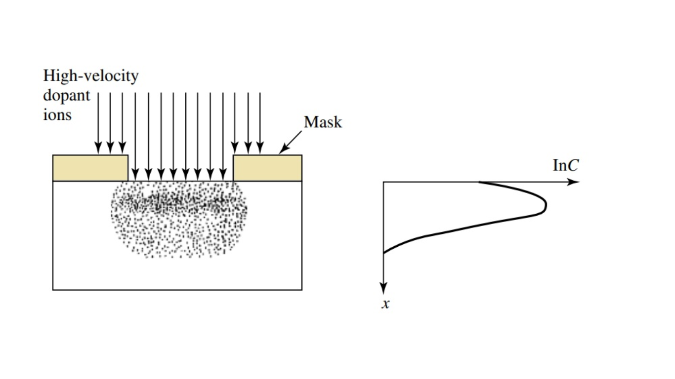
Ion implantation
After that, doping operations have been performed chiefly by ion implantation, as shown in Figure 2. In this process, the dopant ions are implanted into the semiconductor by means of an ion beam. The doping concentration has a peak distribution inside the semiconductor and the profile of the dopant distribution is determined mainly by the ion mass and the implanted ion energy.