
Etching
Etching is the process of creating patterns on a metal plate, glass, or another surface by the corrosive action of an acid. In the manufacture of chips, the chemical removal of material known as etching is frequently repeated for different materials. It’s important to use etchants that remove material selectively, meaning they shouldn’t etch away other materials or only do so very weakly.
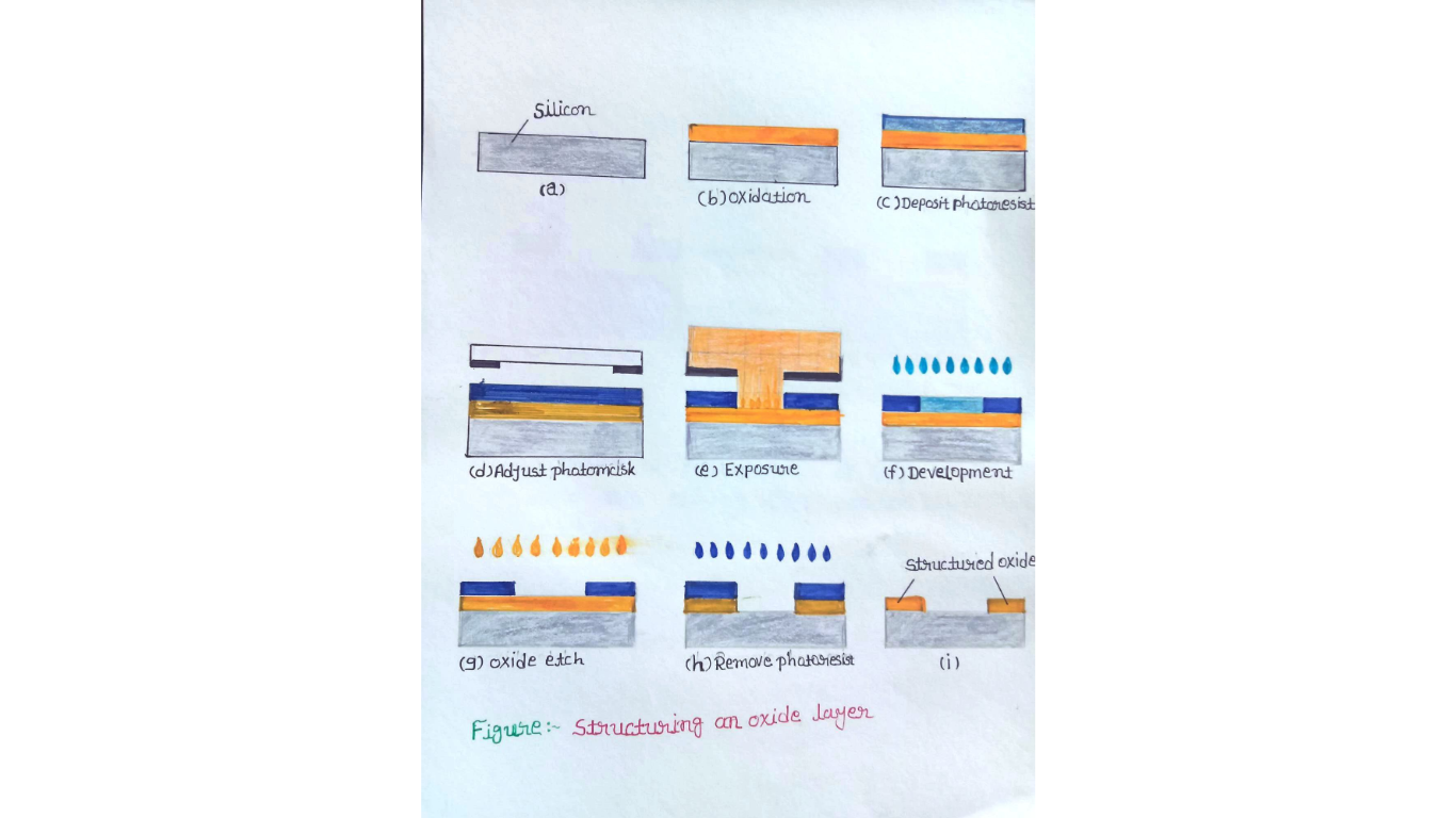
The following figure shows how an existing oxide layer is structured by etching. A photoresist is impervious to etching and is exposed and developed through a photomask. We will discuss here two different types of etching wet etching and dry etching.
Wet etching
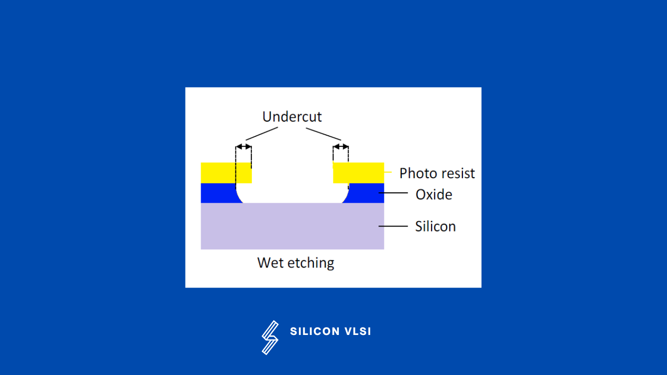
Wet etching is a simple and commonly used method and the fast etching rate we can get. Wet etching, is a material removal process that uses liquid chemicals or etchants to remove materials from a wafer, or oxide is dissolved and removed by a fluid chemical etching agent. The disadvantage of wet etching is that the etching is isotropic, which means its etch in all directions. Because of this, unwanted lateral etching leads to an edge shift as shown in the following figure.
The undercut has a slightly lower etching rate than the vertical etching, as the etching agent cannot circulate as easily under the photoresist and is, therefore, more highly saturated. underneath the photoresist. These so-called undercuts mean that the oxide openings are always bigger than the openings in the photoresist. Wet etching is not appropriate anymore for imaging typical feature sizes in advanced processes, due to this undercutting effect. So, wet etching is only used in these processes for dissolving and removing entire layers.
Advantages wet etching
- It is cheap.
- It is highly selective.
- It has almost no damage due to its purely chemical nature.
Disadvantages wet etching
- It has poor anisotropy.
- It has poor process control and poor particle control,
- Has high chemical disposal costs and is difficult to use with small features
Dry Etching
Dry etching is also called Reactive ion etching (RIE). Dry etching is a more flexible process than wet etching. Plasma Etching is a dry etching method that is the best way to clean a surface before modification. It removes any unwanted organic residues. The ions are set in oscillatory motion via an electrically alternating field. The field is aligned normally with the wafer surface.
The chemically active ions oscillate in this direction and etch away material vertically only. There is no edge shift in this process, which is the main advantage of Dry Etching. Very fine structures can be created with the Dry etching(RIE), process. Furthermore, the resulting trenches can be far deeper than they are wide.

What is the advantage of dry etching over wet etching?
Wet etching requires large amounts of chemicals, is less safe, and offers less control over the etch, on the other hand, Dry etching offers strong isotropic control, more precision, and is generally safer. Dry etching can also, depending on the process, offer a high etch rate, and it uses fewer chemicals.
Where is dry etching used?
A common technique for creating printed circuit boards is dry etching (PCBs). Any exposed surface will be bombarded by and eroded by the plasma’s ions. The photoresist shields the material, allowing the plasma to etch away the exposed portions. #
What is the purpose of etching in semiconductor manufacturing, and how is it used to create patterns?
Etching is used in semiconductor manufacturing to selectively remove material and create patterns such as wires and contact holes on a wafer’s surface. It allows for precise shaping and structuring of the semiconductor material.